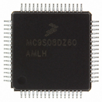
MC9S08DZ60MLC Freescale Semiconductor, MC9S08DZ60MLC Datasheet - Page 86

MC9S08DZ60MLC
Manufacturer Part Number
MC9S08DZ60MLC
Description
IC MCU 60K FLASH 4K RAM 32-LQFP
Manufacturer
Freescale Semiconductor
Series
HCS08r
Specifications of MC9S08DZ60MLC
Core Processor
HCS08
Core Size
8-Bit
Speed
40MHz
Connectivity
CAN, I²C, LIN, SCI, SPI
Peripherals
LVD, POR, PWM, WDT
Number Of I /o
25
Program Memory Size
60KB (60K x 8)
Program Memory Type
FLASH
Eeprom Size
2K x 8
Ram Size
4K x 8
Voltage - Supply (vcc/vdd)
2.7 V ~ 5.5 V
Data Converters
A/D 10x12b
Oscillator Type
External
Operating Temperature
-40°C ~ 125°C
Package / Case
32-LQFP
For Use With
DEMO9S08DZ60 - BOARD DEMOEVB9S08DZ60 - BOARD EVAL FOR 9S08DZ60
Lead Free Status / RoHS Status
Lead free / RoHS Compliant
Available stocks
Company
Part Number
Manufacturer
Quantity
Price
Company:
Part Number:
MC9S08DZ60MLC
Manufacturer:
Freescale Semiconductor
Quantity:
10 000
- Current page: 86 of 416
- Download datasheet (5Mb)
Chapter 6 Parallel Input/Output Control
In general, whenever a pin is shared with both an alternate digital function and an analog function, the
analog function has priority such that if both the digital and analog functions are enabled, the analog
function controls the pin.
It is a good programming practice to write to the port data register before changing the direction of a port
pin to become an output. This ensures that the pin will not be driven momentarily with an old data value
that happened to be in the port data register.
6.2
Associated with the parallel I/O ports is a set of registers located in the high page register space that operate
independently of the parallel I/O registers. These registers are used to control pull-ups, slew rate, and drive
strength for the pins.
An internal pull-up device can be enabled for each port pin by setting the corresponding bit in the pull-up
enable register (PTxPEn). The pull-up device is disabled if the pin is configured as an output by the parallel
I/O control logic or any shared peripheral function regardless of the state of the corresponding pull-up
enable register bit. The pull-up device is also disabled if the pin is controlled by an analog function.
Slew rate control can be enabled for each port pin by setting the corresponding bit in the slew rate control
register (PTxSEn). When enabled, slew control limits the rate at which an output can transition in order to
reduce EMC emissions. Slew rate control has no effect on pins that are configured as inputs.
86
Pull-up, Slew Rate, and Drive Strength
Slew rate reset default values may differ between engineering samples and
final production parts. Always initialize slew rate control to the desired
value to ensure correct operation.
Port Read
BUSCLK
Data
Figure 6-1. Parallel I/O Block Diagram
MC9S08DZ60 Series Data Sheet, Rev. 4
PTxDDn
D
D
PTxDn
Q
Q
NOTE
1
0
Synchronizer
Output Enable
Output Data
Freescale Semiconductor
Input Data
Related parts for MC9S08DZ60MLC
Image
Part Number
Description
Manufacturer
Datasheet
Request
R
Part Number:
Description:
Manufacturer:
Freescale Semiconductor, Inc
Datasheet:
Part Number:
Description:
Manufacturer:
Freescale Semiconductor, Inc
Datasheet:
Part Number:
Description:
Manufacturer:
Freescale Semiconductor, Inc
Datasheet:
Part Number:
Description:
Manufacturer:
Freescale Semiconductor, Inc
Datasheet:
Part Number:
Description:
Manufacturer:
Freescale Semiconductor, Inc
Datasheet:
Part Number:
Description:
Manufacturer:
Freescale Semiconductor, Inc
Datasheet:
Part Number:
Description:
Manufacturer:
Freescale Semiconductor, Inc
Datasheet:
Part Number:
Description:
Manufacturer:
Freescale Semiconductor, Inc
Datasheet:
Part Number:
Description:
Manufacturer:
Freescale Semiconductor, Inc
Datasheet:
Part Number:
Description:
Manufacturer:
Freescale Semiconductor, Inc
Datasheet:
Part Number:
Description:
Manufacturer:
Freescale Semiconductor, Inc
Datasheet:
Part Number:
Description:
Manufacturer:
Freescale Semiconductor, Inc
Datasheet:
Part Number:
Description:
Manufacturer:
Freescale Semiconductor, Inc
Datasheet:
Part Number:
Description:
Manufacturer:
Freescale Semiconductor, Inc
Datasheet:
Part Number:
Description:
Manufacturer:
Freescale Semiconductor, Inc
Datasheet:


