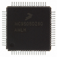
MC9S08DZ60MLC Freescale Semiconductor, MC9S08DZ60MLC Datasheet - Page 87

MC9S08DZ60MLC
Manufacturer Part Number
MC9S08DZ60MLC
Description
IC MCU 60K FLASH 4K RAM 32-LQFP
Manufacturer
Freescale Semiconductor
Series
HCS08r
Specifications of MC9S08DZ60MLC
Core Processor
HCS08
Core Size
8-Bit
Speed
40MHz
Connectivity
CAN, I²C, LIN, SCI, SPI
Peripherals
LVD, POR, PWM, WDT
Number Of I /o
25
Program Memory Size
60KB (60K x 8)
Program Memory Type
FLASH
Eeprom Size
2K x 8
Ram Size
4K x 8
Voltage - Supply (vcc/vdd)
2.7 V ~ 5.5 V
Data Converters
A/D 10x12b
Oscillator Type
External
Operating Temperature
-40°C ~ 125°C
Package / Case
32-LQFP
For Use With
DEMO9S08DZ60 - BOARD DEMOEVB9S08DZ60 - BOARD EVAL FOR 9S08DZ60
Lead Free Status / RoHS Status
Lead free / RoHS Compliant
Available stocks
Company
Part Number
Manufacturer
Quantity
Price
Company:
Part Number:
MC9S08DZ60MLC
Manufacturer:
Freescale Semiconductor
Quantity:
10 000
- Current page: 87 of 416
- Download datasheet (5Mb)
An output pin can be selected to have high output drive strength by setting the corresponding bit in the
drive strength select register (PTxDSn). When high drive is selected, a pin is capable of sourcing and
sinking greater current. Even though every I/O pin can be selected as high drive, the user must ensure that
the total current source and sink limits for the MCU are not exceeded. Drive strength selection is intended
to affect the DC behavior of I/O pins. However, the AC behavior is also affected. High drive allows a pin
to drive a greater load with the same switching speed as a low drive enabled pin into a smaller load.
Because of this, the EMC emissions may be affected by enabling pins as high drive.
6.3
Port A, port B, and port D pins can be configured as external interrupt inputs and as an external means of
waking the MCU from stop or wait low-power modes.
The block diagram for each port interrupt logic is shown
Writing to the PTxPSn bits in the port interrupt pin select register (PTxPS) independently enables or
disables each port pin. Each port can be configured as edge sensitive or edge and level sensitive based on
the PTxMOD bit in the port interrupt status and control register (PTxSC). Edge sensitivity can be software
programmed to be either falling or rising; the level can be either low or high. The polarity of the edge or
edge and level sensitivity is selected using the PTxESn bits in the port interrupt edge select register
(PTxES).
Synchronous logic is used to detect edges. Prior to detecting an edge, enabled port inputs must be at the
deasserted logic level. A falling edge is detected when an enabled port input signal is seen as a logic 1 (the
deasserted level) during one bus cycle and then a logic 0 (the asserted level) during the next cycle. A rising
edge is detected when the input signal is seen as a logic 0 during one bus cycle and then a logic 1 during
the next cycle.
6.3.1
A valid edge on an enabled port pin will set PTxIF in PTxSC. If PTxIE in PTxSC is set, an interrupt request
will be presented to the CPU. Clearing of PTxIF is accomplished by writing a 1 to PTxACK in PTxSC.
Freescale Semiconductor
PTxn
PTxn
PTxES0
PTxESn
Pin Interrupts
1
0
1
0
S
S
Edge Only Sensitivity
PTxPS0
PTxPSn
Figure 6-2. Port Interrupt Block Diagram
MC9S08DZ60 Series Data Sheet, Rev. 4
PTxMOD
V
DD
D
CK
CLR
Q
Figure
INTERRUPT FF
PORT
6-2.
RESET
PTxACK
STOP
Chapter 6 Parallel Input/Output Control
SYNCHRONIZER
STOP BYPASS
BUSCLK
PTxIE
PTxIF
PTx
INTERRUPT
REQUEST
87
Related parts for MC9S08DZ60MLC
Image
Part Number
Description
Manufacturer
Datasheet
Request
R
Part Number:
Description:
Manufacturer:
Freescale Semiconductor, Inc
Datasheet:
Part Number:
Description:
Manufacturer:
Freescale Semiconductor, Inc
Datasheet:
Part Number:
Description:
Manufacturer:
Freescale Semiconductor, Inc
Datasheet:
Part Number:
Description:
Manufacturer:
Freescale Semiconductor, Inc
Datasheet:
Part Number:
Description:
Manufacturer:
Freescale Semiconductor, Inc
Datasheet:
Part Number:
Description:
Manufacturer:
Freescale Semiconductor, Inc
Datasheet:
Part Number:
Description:
Manufacturer:
Freescale Semiconductor, Inc
Datasheet:
Part Number:
Description:
Manufacturer:
Freescale Semiconductor, Inc
Datasheet:
Part Number:
Description:
Manufacturer:
Freescale Semiconductor, Inc
Datasheet:
Part Number:
Description:
Manufacturer:
Freescale Semiconductor, Inc
Datasheet:
Part Number:
Description:
Manufacturer:
Freescale Semiconductor, Inc
Datasheet:
Part Number:
Description:
Manufacturer:
Freescale Semiconductor, Inc
Datasheet:
Part Number:
Description:
Manufacturer:
Freescale Semiconductor, Inc
Datasheet:
Part Number:
Description:
Manufacturer:
Freescale Semiconductor, Inc
Datasheet:
Part Number:
Description:
Manufacturer:
Freescale Semiconductor, Inc
Datasheet:


