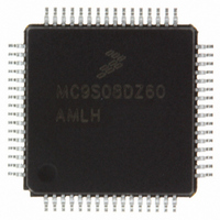
MC9S08DZ60MLC Freescale Semiconductor, MC9S08DZ60MLC Datasheet - Page 152

MC9S08DZ60MLC
Manufacturer Part Number
MC9S08DZ60MLC
Description
IC MCU 60K FLASH 4K RAM 32-LQFP
Manufacturer
Freescale Semiconductor
Series
HCS08r
Specifications of MC9S08DZ60MLC
Core Processor
HCS08
Core Size
8-Bit
Speed
40MHz
Connectivity
CAN, I²C, LIN, SCI, SPI
Peripherals
LVD, POR, PWM, WDT
Number Of I /o
25
Program Memory Size
60KB (60K x 8)
Program Memory Type
FLASH
Eeprom Size
2K x 8
Ram Size
4K x 8
Voltage - Supply (vcc/vdd)
2.7 V ~ 5.5 V
Data Converters
A/D 10x12b
Oscillator Type
External
Operating Temperature
-40°C ~ 125°C
Package / Case
32-LQFP
For Use With
DEMO9S08DZ60 - BOARD DEMOEVB9S08DZ60 - BOARD EVAL FOR 9S08DZ60
Lead Free Status / RoHS Status
Lead free / RoHS Compliant
Available stocks
Company
Part Number
Manufacturer
Quantity
Price
Company:
Part Number:
MC9S08DZ60MLC
Manufacturer:
Freescale Semiconductor
Quantity:
10 000
- Current page: 152 of 416
- Download datasheet (5Mb)
Chapter 8 Multi-Purpose Clock Generator (S08MCGV1)
8.4.7
The MCG presents the divided reference clock as MCGFFCLK for use as an additional clock source. The
MCGFFCLK frequency must be no more than 1/4 of the MCGOUT frequency to be valid. Because of this
requirement, the MCGFFCLK is not valid in bypass modes for the following combinations of BDIV and
RDIV values:
When MCGFFCLK is valid then MCGFFCLKVALID is set to 1. When MCGFFCLK is not valid then
MCGFFCLKVALID is set to 0.
8.5
This section describes how to initialize and configure the MCG module in application. The following
sections include examples on how to initialize the MCG and properly switch between the various available
modes.
8.5.1
The MCG comes out of reset configured for FEI mode with the BDIV set for divide-by-2. The internal
reference will stabilize in t
reference is stable, the FLL will acquire lock in t
Upon POR, the internal reference will require trimming to guarantee an accurate clock. Freescale
recommends using FLASH location 0xFFAE for storing the fine trim bit, FTRIM in the MCGSC register,
and 0xFFAF for storing the 8-bit trim value in the MCGTRM register. The MCU will not automatically
copy the values in these FLASH locations to the respective registers. Therefore, user code must copy these
values from FLASH to the registers.
8.5.1.1
Because the MCG comes out of reset in FEI mode, the only MCG modes which can be directly switched
to upon reset are FEE, FBE, and FBI modes (see
first configuring the MCG for one of these three initial modes. Care must be taken to check relevant status
bits in the MCGSC register reflecting all configuration changes within each mode.
To change from FEI mode to FEE or FBE modes, follow this procedure:
152
1. Enable the external clock source by setting the appropriate bits in MCGC2.
2. Write to MCGC1 to select the clock mode.
Initialization / Application Information
Fixed Frequency Clock
MCG Module Initialization Sequence
Initializing the MCG
•
•
The BDIV value should not be changed to divide-by-1 without first
trimming the internal reference. Failure to do so could result in the MCU
running out of specification.
BDIV=00 (divide by 1), RDIV < 010
BDIV=01 (divide by 2), RDIV < 011
irefst
microseconds before the FLL can acquire lock. As soon as the internal
MC9S08DZ60 Series Data Sheet, Rev. 4
fll_lock
NOTE
Figure
milliseconds.
8-8). Reaching any of the other modes requires
Freescale Semiconductor
Related parts for MC9S08DZ60MLC
Image
Part Number
Description
Manufacturer
Datasheet
Request
R
Part Number:
Description:
Manufacturer:
Freescale Semiconductor, Inc
Datasheet:
Part Number:
Description:
Manufacturer:
Freescale Semiconductor, Inc
Datasheet:
Part Number:
Description:
Manufacturer:
Freescale Semiconductor, Inc
Datasheet:
Part Number:
Description:
Manufacturer:
Freescale Semiconductor, Inc
Datasheet:
Part Number:
Description:
Manufacturer:
Freescale Semiconductor, Inc
Datasheet:
Part Number:
Description:
Manufacturer:
Freescale Semiconductor, Inc
Datasheet:
Part Number:
Description:
Manufacturer:
Freescale Semiconductor, Inc
Datasheet:
Part Number:
Description:
Manufacturer:
Freescale Semiconductor, Inc
Datasheet:
Part Number:
Description:
Manufacturer:
Freescale Semiconductor, Inc
Datasheet:
Part Number:
Description:
Manufacturer:
Freescale Semiconductor, Inc
Datasheet:
Part Number:
Description:
Manufacturer:
Freescale Semiconductor, Inc
Datasheet:
Part Number:
Description:
Manufacturer:
Freescale Semiconductor, Inc
Datasheet:
Part Number:
Description:
Manufacturer:
Freescale Semiconductor, Inc
Datasheet:
Part Number:
Description:
Manufacturer:
Freescale Semiconductor, Inc
Datasheet:
Part Number:
Description:
Manufacturer:
Freescale Semiconductor, Inc
Datasheet:


