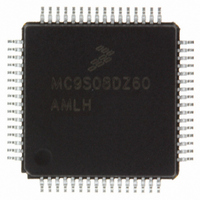
MC9S08DZ60MLC Freescale Semiconductor, MC9S08DZ60MLC Datasheet - Page 81

MC9S08DZ60MLC
Manufacturer Part Number
MC9S08DZ60MLC
Description
IC MCU 60K FLASH 4K RAM 32-LQFP
Manufacturer
Freescale Semiconductor
Series
HCS08r
Specifications of MC9S08DZ60MLC
Core Processor
HCS08
Core Size
8-Bit
Speed
40MHz
Connectivity
CAN, I²C, LIN, SCI, SPI
Peripherals
LVD, POR, PWM, WDT
Number Of I /o
25
Program Memory Size
60KB (60K x 8)
Program Memory Type
FLASH
Eeprom Size
2K x 8
Ram Size
4K x 8
Voltage - Supply (vcc/vdd)
2.7 V ~ 5.5 V
Data Converters
A/D 10x12b
Oscillator Type
External
Operating Temperature
-40°C ~ 125°C
Package / Case
32-LQFP
For Use With
DEMO9S08DZ60 - BOARD DEMOEVB9S08DZ60 - BOARD EVAL FOR 9S08DZ60
Lead Free Status / RoHS Status
Lead free / RoHS Compliant
Available stocks
Company
Part Number
Manufacturer
Quantity
Price
Company:
Part Number:
MC9S08DZ60MLC
Manufacturer:
Freescale Semiconductor
Quantity:
10 000
- Current page: 81 of 416
- Download datasheet (5Mb)
1
5.8.5
This high page register contains bits to configure MCU specific features on the MC9S08DZ60 Series
devices.
Freescale Semiconductor
This bit can be written only one time after reset. Additional writes are ignored.
COPCLKS
Reset:
ADHTS
MCSEL
COPW
Field
2:0
7
6
4
W
R
COPCLKS
System Options Register 2 (SOPT2)
COP Watchdog Clock Select — This write-once bit selects the clock source of the COP watchdog. See
Table 5-6
0 Internal 1-kHz clock is source to COP.
1 Bus clock is source to COP.
COP Window — This write-once bit selects the COP operation mode. When set, the 0x55-0xAA write sequence
to the SRS register must occur in the last 25% of the selected period. Any write to the SRS register during the
first 75% of the selected period will reset the MCU.
0 Normal COP operation.
1 Window COP operation.
ADC Hardware Trigger Select — This bit selects which hardware trigger initiates conversion for the analog to
digital converter when the ADC hardware trigger is enabled (ADCTRG is set in ADCSC2 register).
0 Real Time Counter (RTC) overflow.
1 External Interrupt Request (IRQ) pin.
MCLK Divide Select— These bits enable the MCLK output on PTA0 pin and select the divide ratio for the MCLK
output according to the formula below when the MCSEL bits are not equal to all zeroes. In case that the MCSEL
bits are all zeroes, the MCLK output is disabled.
0
7
1
= Unimplemented or Reserved
for details.
COPW
0
6
1
Figure 5-6. System Options Register 2 (SOPT2)
Table 5-7. SOPT2 Register Field Descriptions
MCLK frequency = Bus Clock frequency ÷ (2 * MCSEL)
MC9S08DZ60 Series Data Sheet, Rev. 4
0
0
5
ADHTS
0
4
Description
Chapter 5 Resets, Interrupts, and General System Control
3
0
0
0
2
MCSEL
0
1
0
0
81
Related parts for MC9S08DZ60MLC
Image
Part Number
Description
Manufacturer
Datasheet
Request
R
Part Number:
Description:
Manufacturer:
Freescale Semiconductor, Inc
Datasheet:
Part Number:
Description:
Manufacturer:
Freescale Semiconductor, Inc
Datasheet:
Part Number:
Description:
Manufacturer:
Freescale Semiconductor, Inc
Datasheet:
Part Number:
Description:
Manufacturer:
Freescale Semiconductor, Inc
Datasheet:
Part Number:
Description:
Manufacturer:
Freescale Semiconductor, Inc
Datasheet:
Part Number:
Description:
Manufacturer:
Freescale Semiconductor, Inc
Datasheet:
Part Number:
Description:
Manufacturer:
Freescale Semiconductor, Inc
Datasheet:
Part Number:
Description:
Manufacturer:
Freescale Semiconductor, Inc
Datasheet:
Part Number:
Description:
Manufacturer:
Freescale Semiconductor, Inc
Datasheet:
Part Number:
Description:
Manufacturer:
Freescale Semiconductor, Inc
Datasheet:
Part Number:
Description:
Manufacturer:
Freescale Semiconductor, Inc
Datasheet:
Part Number:
Description:
Manufacturer:
Freescale Semiconductor, Inc
Datasheet:
Part Number:
Description:
Manufacturer:
Freescale Semiconductor, Inc
Datasheet:
Part Number:
Description:
Manufacturer:
Freescale Semiconductor, Inc
Datasheet:
Part Number:
Description:
Manufacturer:
Freescale Semiconductor, Inc
Datasheet:


