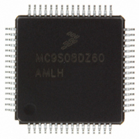
MC9S08DZ60MLC Freescale Semiconductor, MC9S08DZ60MLC Datasheet - Page 252

MC9S08DZ60MLC
Manufacturer Part Number
MC9S08DZ60MLC
Description
IC MCU 60K FLASH 4K RAM 32-LQFP
Manufacturer
Freescale Semiconductor
Series
HCS08r
Specifications of MC9S08DZ60MLC
Core Processor
HCS08
Core Size
8-Bit
Speed
40MHz
Connectivity
CAN, I²C, LIN, SCI, SPI
Peripherals
LVD, POR, PWM, WDT
Number Of I /o
25
Program Memory Size
60KB (60K x 8)
Program Memory Type
FLASH
Eeprom Size
2K x 8
Ram Size
4K x 8
Voltage - Supply (vcc/vdd)
2.7 V ~ 5.5 V
Data Converters
A/D 10x12b
Oscillator Type
External
Operating Temperature
-40°C ~ 125°C
Package / Case
32-LQFP
For Use With
DEMO9S08DZ60 - BOARD DEMOEVB9S08DZ60 - BOARD EVAL FOR 9S08DZ60
Lead Free Status / RoHS Status
Lead free / RoHS Compliant
Available stocks
Company
Part Number
Manufacturer
Quantity
Price
Company:
Part Number:
MC9S08DZ60MLC
Manufacturer:
Freescale Semiconductor
Quantity:
10 000
- Current page: 252 of 416
- Download datasheet (5Mb)
Chapter 12 Freescale’s Controller Area Network (S08MSCANV1)
12.5.2.1
Modern application layer software is built upon two fundamental assumptions:
The behavior described in the bullets above cannot be achieved with a single transmit buffer. That buffer
must be reloaded immediately after the previous message is sent. This loading process lasts a finite amount
of time and must be completed within the inter-frame sequence (IFS) to be able to send an uninterrupted
stream of messages. Even if this is feasible for limited CAN bus speeds, it requires that the CPU reacts
with short latencies to the transmit interrupt.
A double buffer scheme de-couples the reloading of the transmit buffer from the actual message sending
and, therefore, reduces the reactiveness requirements of the CPU. Problems can arise if the sending of a
message is finished while the CPU re-loads the second buffer. No buffer would then be ready for
transmission, and the CAN bus would be released.
At least three transmit buffers are required to meet the first of the above requirements under all
circumstances. The MSCAN has three transmit buffers.
The second requirement calls for some sort of internal prioritization which the MSCAN implements with
the “local priority” concept described in
12.5.2.2
The MSCAN triple transmit buffer scheme optimizes real-time performance by allowing multiple
messages to be set up in advance. The three buffers are arranged as shown in
All three buffers have a 13-byte data structure similar to the outline of the receive buffers (see
“Programmer’s Model of Message
Register (TBPR)
Priority Register
(see
To transmit a message, the CPU must identify an available transmit buffer, which is indicated by a set
transmitter buffer empty (TXEx) flag (see
(CANTFLG)”). If a transmit buffer is available, the CPU must set a pointer to this buffer by writing to the
CANTBSEL register (see
(CANTBSEL)”). This makes the respective buffer accessible within the CANTXFG address space (see
Section 12.4, “Programmer’s Model of Message
CANTBSEL register simplifies the transmit buffer selection. In addition, this scheme makes the handler
software simpler because only one address area is applicable for the transmit process, and the required
address space is minimized.
The CPU then stores the identifier, the control bits, and the data content into one of the transmit buffers.
Finally, the buffer is flagged as ready for transmission by clearing the associated TXE flag.
252
•
•
Section 12.4.6, “Time Stamp Register
Any CAN node is able to send out a stream of scheduled messages without releasing the CAN bus
between the two messages. Such nodes arbitrate for the CAN bus immediately after sending the
previous message and only release the CAN bus in case of lost arbitration.
The internal message queue within any CAN node is organized such that the highest priority
message is sent out first, if more than one message is ready to be sent.
Message Transmit Background
Transmit Structures
(TBPR)”). The remaining two bytes are used for time stamping of a message, if required
contains an 8-bit local priority field (PRIO) (see
Section 12.3.10, “MSCAN Transmit Buffer Selection Register
Storage”). An additional
MC9S08DZ60 Series Data Sheet, Rev. 4
Section 12.5.2.2, “Transmit
Section 12.3.6, “MSCAN Transmitter Flag Register
(TSRH–TSRL)”).
Storage”). The algorithmic feature associated with the
Section 12.4.5, “Transmit Buffer Priority
Section 12.4.5, “Transmit Buffer
Structures.”
Figure
Freescale Semiconductor
12-38.
Section 12.4,
Related parts for MC9S08DZ60MLC
Image
Part Number
Description
Manufacturer
Datasheet
Request
R
Part Number:
Description:
Manufacturer:
Freescale Semiconductor, Inc
Datasheet:
Part Number:
Description:
Manufacturer:
Freescale Semiconductor, Inc
Datasheet:
Part Number:
Description:
Manufacturer:
Freescale Semiconductor, Inc
Datasheet:
Part Number:
Description:
Manufacturer:
Freescale Semiconductor, Inc
Datasheet:
Part Number:
Description:
Manufacturer:
Freescale Semiconductor, Inc
Datasheet:
Part Number:
Description:
Manufacturer:
Freescale Semiconductor, Inc
Datasheet:
Part Number:
Description:
Manufacturer:
Freescale Semiconductor, Inc
Datasheet:
Part Number:
Description:
Manufacturer:
Freescale Semiconductor, Inc
Datasheet:
Part Number:
Description:
Manufacturer:
Freescale Semiconductor, Inc
Datasheet:
Part Number:
Description:
Manufacturer:
Freescale Semiconductor, Inc
Datasheet:
Part Number:
Description:
Manufacturer:
Freescale Semiconductor, Inc
Datasheet:
Part Number:
Description:
Manufacturer:
Freescale Semiconductor, Inc
Datasheet:
Part Number:
Description:
Manufacturer:
Freescale Semiconductor, Inc
Datasheet:
Part Number:
Description:
Manufacturer:
Freescale Semiconductor, Inc
Datasheet:
Part Number:
Description:
Manufacturer:
Freescale Semiconductor, Inc
Datasheet:


