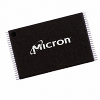
MT29F8G08BAAWP:A TR Micron Technology Inc, MT29F8G08BAAWP:A TR Datasheet - Page 26

MT29F8G08BAAWP:A TR
Manufacturer Part Number
MT29F8G08BAAWP:A TR
Description
IC FLASH 8GBIT 48TSOP
Manufacturer
Micron Technology Inc
Datasheet
1.MT29F16G08DAAWP-ETA_TR.pdf
(81 pages)
Specifications of MT29F8G08BAAWP:A TR
Format - Memory
FLASH
Memory Type
FLASH - Nand
Memory Size
8G (1G x 8)
Interface
Parallel
Voltage - Supply
2.7 V ~ 3.6 V
Operating Temperature
0°C ~ 70°C
Package / Case
48-TSOP
Lead Free Status / RoHS Status
Lead free / RoHS Compliant
Speed
-
READ STATUS 70h
Table 9:
PDF: 09005aef81b80e13/Source: 09005aef81b80eac
4gb_nand_m40a__2.fm - Rev. B 2/07 EN
Bit
SR
0
1
2
3
4
5
6
7
1
Write protect
Ready/busy
Ready/busy
Program
Pass/fail
Page
Status Register Bit Definition
–
–
–
–
Notes:
Program Page
Cache Mode
Pass/fail (N-1)
Write protect
Ready/busy
Pass/fail (N)
Ready/busy
cache
These NAND Flash devices have an 8-bit status register the software can read during
device operation. Table 9 describes the status register.
After a READ STATUS command, all READ cycles will be from the status register until a
new command is issued. Changes in the status register will be seen on I/O[7:0] as long
as CE# and RE# are LOW; it is not necessary to start a new READ STATUS cycle to see
these changes.
In devices that have more than one die sharing a common CE# pin, the READ STATUS
(70h) command reports the status of the die that was last addressed. If interleaved oper-
ations are started on both die, then the TWO-PLANE/MULTIPLE-DIE READ STATUS
(78h) command must be used to select the die that should report status. In this situa-
tion, using the READ STATUS (70h) command will result in bus contention, as both die
will respond until the next operation is issued.
While monitoring the status register to determine when the
Flash array to data register) is complete, the user must reissue the READ (00h) command
to make the change from status to read mode. After the READ command has been reis-
sued, pulsing the RE# line will result in outputting data, starting from the initial column
address.
1. Status register bit 0 reports a “1” if a TWO-PLANE PROGRAM PAGE or TWO-PLANE BLOCK
2. Status register bit 5 is “0” during the actual programming operation. If cache mode is used,
3. Status register bit 6 is “1” when the cache is ready to accept new data. R/B# follows bit 6.
–
–
–
ERASE operation fails on one or both planes. Status register bit 1 reports a “1” if a TWO-
PLANE PROGRAM PAGE CACHE MODE operation fails on one or both planes. Use TWO-
PLANE/MULTIPLE-DIE READ STATUS (78h) to determine the plane to which the operation
failed.
this bit will be “1” when all internal operations are complete.
See Figure 19 on page 29 and Figure 73 on page 77.
3
2
Write protect Write protect
Page Read
Ready/busy
Ready/busy
–
–
–
–
–
Cache Mode
Ready/busy
Page Read
Ready/busy
cache
26
4Gb, 8Gb, and 16Gb x8 NAND Flash Memory
–
–
–
–
–
3
2
Micron Technology, Inc., reserves the right to change products or specifications without notice.
Write protect 0 = Protected
Block Erase
Ready/busy
Ready/busy
Pass/fail
–
–
–
–
0 = Successful PROGRAM/ERASE
1 = Error in PROGRAM/ERASE
0 = Successful PROGRAM
1 = Error in PROGRAM
0
0
0
0 = Busy
1 = Ready
0 = Busy
1 = Ready
1 = Not protected
Command Definitions
t
R (transfer from NAND
©2006 Micron Technology, Inc. All rights reserved.
Definition


