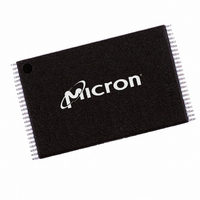
MT29F8G08BAAWP:A TR Micron Technology Inc, MT29F8G08BAAWP:A TR Datasheet - Page 40

MT29F8G08BAAWP:A TR
Manufacturer Part Number
MT29F8G08BAAWP:A TR
Description
IC FLASH 8GBIT 48TSOP
Manufacturer
Micron Technology Inc
Datasheet
1.MT29F16G08DAAWP-ETA_TR.pdf
(81 pages)
Specifications of MT29F8G08BAAWP:A TR
Format - Memory
FLASH
Memory Type
FLASH - Nand
Memory Size
8G (1G x 8)
Interface
Parallel
Voltage - Supply
2.7 V ~ 3.6 V
Operating Temperature
0°C ~ 70°C
Package / Case
48-TSOP
Lead Free Status / RoHS Status
Lead free / RoHS Compliant
Speed
-
Figure 29:
TWO-PLANE PROGRAM PAGE CACHE MODE 80h-11h-80h-15h
PDF: 09005aef81b80e13/Source: 09005aef81b80eac
4gb_nand_m40a__2.fm - Rev. B 2/07 EN
R/B#
R/B#
I/Ox
I/Ox
80h
1
85h
Address (5 cycles)
1st plane address
Repeat as many times as necessary
TWO-PLANE PROGRAM PAGE Operation with RANDOM DATA INPUT
address than previous
5 address cycles, for
Different column
Address (2 cycles)
2nd plane only
Data
The TWO-PLANE PROGRAM PAGE CACHE MODE (80h-11h-80h-15h) operation is
similar to the PROGRAM PAGE CACHE MODE (80h-15h) operation. It programs two
pages of data from the data registers to the NAND Flash arrays. The pages must be
programmed to different planes on the same die. Within a block, the pages must be
programmed consecutively from the least significant to the most significant page
address. Random page programming within a block is prohibited. The first-plane and
second-plane addresses must meet the two-plane addressing requirements (see “Two-
Plane Addressing” on page 35).
To enter the two-plane program page cache mode, write the 80h command to the
command register, write 5 ADDRESS cycles for the first plane, then write the data. Serial
data is loaded on consecutive WE# cycles starting at the given address. Next, write the
11h command. The 11h command is a “dummy” command that informs the control
logic that the first set of data for the first plane is complete. No programming of the
NAND Flash array occurs. R/B# goes LOW for
STATUS (70h) command also indicates that the device is ready when status register bit 6
is set to “1.” The only valid commands during
(FFh).
After
ADDRESS cycles for the second plane, then write the data. The CACHE WRITE (15h)
command is written after the second-plane data input is complete. Data is transferred
from the cache registers to the data registers on the rising edge of WE#. R/B# goes LOW
during this transfer time. After the data has been copied into the data registers and R/B#
returns HIGH, memory array programming to both planes begins.
Data
input
t
DBSY, write the 80h (or 81h) command to the command register, write 5
input
85h
Repeat as many times as necessary
address than previous
5 address cycles, for
10h
Different column
Address (2 cycles)
1st plane only
t PROG
40
4Gb, 8Gb, and 16Gb x8 NAND Flash Memory
Data
input
Micron Technology, Inc., reserves the right to change products or specifications without notice.
11h
t
t
DBSY are READ STATUS (70h) and RESET
DBSY, then returns HIGH. The READ
t DBSY
(or 81h)
80h
2nd plane address
Address (5 cycles)
Command Definitions
©2006 Micron Technology, Inc. All rights reserved.
Data
input
1


