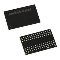
W9751G6IB-25 Winbond Electronics, W9751G6IB-25 Datasheet - Page 10

W9751G6IB-25
Manufacturer Part Number
W9751G6IB-25
Description
IC DDR2-800 SDRAM 512MB 84-WBGA
Manufacturer
Winbond Electronics
Datasheet
1.W9751G6IB-25.pdf
(86 pages)
Specifications of W9751G6IB-25
Format - Memory
RAM
Memory Type
DDR2 SDRAM
Memory Size
512M (32Mx16)
Speed
2.5ns
Interface
Parallel
Voltage - Supply
1.7 V ~ 1.9 V
Operating Temperature
0°C ~ 85°C
Package / Case
84-WBGA
Lead Free Status / RoHS Status
Lead free / RoHS Compliant
Available stocks
Company
Part Number
Manufacturer
Quantity
Price
Company:
Part Number:
W9751G6IB-25
Manufacturer:
WINBOND
Quantity:
15
Company:
Part Number:
W9751G6IB-25
Manufacturer:
WINBOND
Quantity:
1 248
Company:
Part Number:
W9751G6IB-25
Manufacturer:
Winbond Electronics
Quantity:
10 000
Part Number:
W9751G6IB-25
Manufacturer:
WINBOND/华邦
Quantity:
20 000
Notes:
1. To guarantee ODT off, V
2. V
3. V
4. The V
7.2
For application flexibility, burst length, burst type, CAS Latency, DLL reset function, write recovery
time (WR) are user defined variables and must be programmed with a Mode Register Set (MRS)
command. Additionally, DLL disable function, driver impedance, additive CAS Latency, ODT (On Die
Termination), single-ended strobe and OCD (off chip driver impedance adjustment) are also user
defined variables and must be programmed with an Extended Mode Register Set (EMRS) command.
Contents of the Mode Register (MR) or Extended Mode Registers EMR (1), EMR (2) and EMR (3) can
be altered by re-executing the MRS or EMRS Commands. Even if the user chooses to modify only a
subset of the MR or EMR (1), EMR (2) and EMR (3) variables, all variables within the addressed
register must be redefined when the MRS or EMRS commands are issued.
MRS, EMRS and Reset DLL do not affect array contents, which mean re-initialization including those
can be executed at any time after power-up without affecting array contents.
7.2.1
( CS = "L", RAS = "L", CAS = "L", WE = "L", BA0 = "L", BA1 = "L", A0 to A12 = Register Data)
The mode register stores the data for controlling the various operating modes of DDR2 SDRAM. It
programs CAS Latency, burst length, burst sequence, test mode, DLL reset, Write Recovery (WR) and
various vendor specific options to make DDR2 SDRAM useful for various applications. The default
value in the Mode Register after power-up is not defined, therefore the Mode Register must be
programmed during initialization for proper operation.
The DDR2 SDRAM should be in all bank precharge state with CKE already HIGH prior to writing into
the mode register. The mode register set command cycle time (t
operation to the mode register. The mode register contents can be changed using the same command
and clock cycle requirements during normal operation as long as all banks are in the precharge state.
The mode register is divided into various fields depending on functionality. Burst length is defined by
A[2:0] with options of 4 and 8 bit burst lengths. The burst length decodes are compatible with DDR
greater than 500 mS.
REF
DD
/V
CKE
ODT
Command
CLK
CLK
Mode Register and Extended Mode Registers Operation
must be within ± 300 mV with respect to V
DDQ
DDL
Mode Register Set Command (MRS)
voltage ramp time must be no greater than 200 mS from when V
voltage ramp time from when V
t
CH
t
IS
t
NOP
CL
400nS
PRE
REF
ALL
Figure 1—Initialization sequence after power-up
t
must be valid and a LOW level must be applied to the ODT pin.
RP
EMRS
DLL
Enable
t
MRD
DLL
Reset
MRS
DD
t
MRD
min is achieved on V
DDQ
PRE
ALL
/2 during supply ramp time.
t
RP
REF
- 10 -
t
RFC
DD
min 200 Cycle
REF
to when V
DD
t
RFC
MRD
ramps from 300 mV to V
Publication Release Date: Oct. 23, 2009
DDQ
MRS
) is required to complete the write
min is achieved on V
t
MRD
OCD
Default
EMRS
Follow OCD
Flow chart
W9751G6IB
EMRS
OCD
CAL. Mode
Exit
DD
DDQ
min.
t
OIT
Revision A06
t
must be no
IS
CMD
ANY


