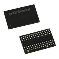
W9751G6IB-25 Winbond Electronics, W9751G6IB-25 Datasheet - Page 41

W9751G6IB-25
Manufacturer Part Number
W9751G6IB-25
Description
IC DDR2-800 SDRAM 512MB 84-WBGA
Manufacturer
Winbond Electronics
Datasheet
1.W9751G6IB-25.pdf
(86 pages)
Specifications of W9751G6IB-25
Format - Memory
RAM
Memory Type
DDR2 SDRAM
Memory Size
512M (32Mx16)
Speed
2.5ns
Interface
Parallel
Voltage - Supply
1.7 V ~ 1.9 V
Operating Temperature
0°C ~ 85°C
Package / Case
84-WBGA
Lead Free Status / RoHS Status
Lead free / RoHS Compliant
Available stocks
Company
Part Number
Manufacturer
Quantity
Price
Company:
Part Number:
W9751G6IB-25
Manufacturer:
WINBOND
Quantity:
15
Company:
Part Number:
W9751G6IB-25
Manufacturer:
WINBOND
Quantity:
1 248
Company:
Part Number:
W9751G6IB-25
Manufacturer:
Winbond Electronics
Quantity:
10 000
Part Number:
W9751G6IB-25
Manufacturer:
WINBOND/华邦
Quantity:
20 000
Notes:
1. V
2. I
3. Input slew rate is specified by AC Parametric Test Condition.
4. I
5. Data Bus consists of DQ, LDM, UDM, LDQS, LDQS , UDQS and UDQS .
6. Definitions for I
I
DD
DD
I
I
DD4W
DD
DD4R
DD5B
I
I
DD6
DD7
LOW = V
HIGH = V
STABLE = inputs stable at a HIGH or LOW level
FLOATING = inputs at V
SWITCHING = inputs changing between HIGH and LOW every other clock cycle (once per two clocks) for address and
specifications are tested after the device is properly initialized.
parameters are specified with ODT disabled.
= 1.8 V
in
±
Operating Burst Read Current
All banks open, Continuous burst reads, I
BL = 4, CL = CL
t
CKE is HIGH, CS is HIGH between valid commands;
Address inputs are SWITCHING;
Data Bus inputs are SWITCHING.
Operating Burst Write Current
All banks open, Continuous burst writes;
BL = 4, CL = CL
t
CKE is HIGH, CS is HIGH between valid commands;
Address inputs are SWITCHING;
Data Bus inputs are SWITCHING.
Burst Refresh Current
t
Refresh command every t
CKE is HIGH, CS is HIGH between valid commands;
Other control and address inputs are SWITCHING;
Data bus inputs are SWITCHING.
Self Refresh Current
CKE ≦ 0.2 V, external clock off, CLK and CLK at 0 V;
Other control and address inputs are FLOATING;
Data bus inputs are FLOATING.
Operating Bank Interleave Read Current
All bank interleaving reads, I
BL = 4, CL = CL
t
t
CKE is HIGH, CS is HIGH between valid commands;
Address bus inputs are STABLE during deselects;
Data Bus inputs are SWITCHING.
in
CK
CK
CK
CK
RCD(IDD)
0.1V; V
≦ V
DD
≧ V
= t
= t
= t
= t
control signals, and inputs changing between HIGH and LOW every other data transfer (once per clock)
for DQ signals not including masks or strobes.
CK(IDD)
CK(IDD)
CK(IDD)
CK(IDD)
IL (ac) (max)
IH (ac) (min)
;
DDQ
; t
; t
;
, t
= 1.8 V
REF
RAS
RAS
RC
(IDD),
(IDD),
(IDD),
= t
= V
= t
= t
±
RC(IDD)
AL = 0;
AL = 0;
AL = t
DDQ
RASmax(IDD)
RASmax(IDD)
0.1V.
RFC(IDD)
/2
RCD(IDD)
OUT
, t
RRD
= 0mA;
interval;
, t
, t
= t
RP
RP
- 1 x t
RRD(IDD)
= t
= t
OUT
CK(IDD)
RP(IDD)
RP(IDD)
= 0 mA;
- 41 -
, t
RCD
;
;
;
=
176
175
135
300
7
Publication Release Date: Oct. 23, 2009
176
175
135
300
7
155
160
125
290
7
W9751G6IB
mA
mA
mA
mA
mA
Revision A06
1,2,3,4,
1,2,3,4,
1,2,3,4,
1,2,3,4,
1,2,3,4,
5,6
5,6
5,6
5,6
5,6


