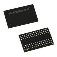
W9751G6IB-25 Winbond Electronics, W9751G6IB-25 Datasheet - Page 54

W9751G6IB-25
Manufacturer Part Number
W9751G6IB-25
Description
IC DDR2-800 SDRAM 512MB 84-WBGA
Manufacturer
Winbond Electronics
Datasheet
1.W9751G6IB-25.pdf
(86 pages)
Specifications of W9751G6IB-25
Format - Memory
RAM
Memory Type
DDR2 SDRAM
Memory Size
512M (32Mx16)
Speed
2.5ns
Interface
Parallel
Voltage - Supply
1.7 V ~ 1.9 V
Operating Temperature
0°C ~ 85°C
Package / Case
84-WBGA
Lead Free Status / RoHS Status
Lead free / RoHS Compliant
Available stocks
Company
Part Number
Manufacturer
Quantity
Price
Company:
Part Number:
W9751G6IB-25
Manufacturer:
WINBOND
Quantity:
15
Company:
Part Number:
W9751G6IB-25
Manufacturer:
WINBOND
Quantity:
1 248
Company:
Part Number:
W9751G6IB-25
Manufacturer:
Winbond Electronics
Quantity:
10 000
Part Number:
W9751G6IB-25
Manufacturer:
WINBOND/华邦
Quantity:
20 000
36. When the device is operated with input clock jitter, this parameter needs to be derated by the actual tJIT(per) of the input
37. When the device is operated with input clock jitter, this parameter needs to be derated by the actual tJIT(duty) of the input
38. When the device is operated with input clock jitter, this parameter needs to be derated by { -tJIT(duty),max - tERR(6-
39. For tAOFD of DDR2-667/800, the 1/2 clock of nCK in the 2.5 x nCK assumes a tCH(avg), average input clock HIGH pulse
Note that these deratings are in addition to the tAOF derating per input clock jitter, i.e. tJIT(duty) and tERR(6-10per). However
tAC values used in the equations shown above are from the timing parameter table and are not derated.
Thus the final derated values for tAOF are;
40. Timings are specified with command/address input slew rate of 1.0 V/nS.
41. Timings are specified with DQs and DM input slew rate of 1.0V/nS.
42. Timings are specified with CLK/ CLK differential slew rate of 2.0 V/nS. Timings are guaranteed for DQS signals with a
clock. (output deratings are relative to the SDRAM input clock.)
clock. (output deratings are relative to the SDRAM input clock.)
10per),max } and { - tJIT(duty),min - tERR(6-10per),min } of the actual input clock. (output deratings are relative to the
SDRAM input clock.)
width of 0.5 relative to tCK(avg). tAOF,min and tAOF,max should each be derated by the same amount as the actual
amount of tCH(avg) offset present at the DRAM input with respect to 0.5.
differential slew rate of 2.0 V/nS in differential strobe mode.
Example:
If the measured jitter into a DDR2-667 SDRAM has tJIT(per),min = - 72 pS and tJIT(per),max = + 93 pS, then
tRPRE,min(derated) = tRPRE,min + tJIT(per),min = 0.9 x tCK(avg) - 72 pS = + 2178 pS and tRPRE,max(derated) =
tRPRE,max + tJIT(per),max = 1.1 x tCK(avg) + 93 pS = + 2843 pS. (Caution on the min/max usage!)
Example:
If the measured jitter into a DDR2-667 SDRAM has tJIT(duty),min = - 72 pS and tJIT(duty),max = + 93 pS, then
tRPST,min(derated) = tRPST,min + tJIT(duty),min = 0.4 x tCK(avg) - 72 pS = + 928 pS and tRPST,max(derated) =
tRPST,max + tJIT(duty),max = 0.6 x tCK(avg) + 93 pS = + 1592 pS. (Caution on the min/max usage!)
Example:
1) If the measured jitter into a DDR2-667 SDRAM has tERR(6-10per),min = - 272 pS, tERR(6-10per),max = + 293
pS, tJIT(duty),min = - 106 pS and tJIT(duty),max = + 94 pS, then tAOF,min(derated) = tAOF,min + { - tJIT(duty),max
- tERR(6-10per),max } = - 450 pS + { - 94 pS - 293 pS} = - 837 pS and tAOF,max(derated) = tAOF,max + { -
tJIT(duty),min - tERR(6-10per),min } = 1050 pS + { 106 pS + 272 pS } = + 1428 pS. (Caution on the min/max
usage!)
Example:
If an input clock has a worst case tCH(avg) of 0.48, the tAOF,min should be derated by subtracting 0.02 x tCK(avg)
from it, whereas if an input clock has a worst case tCH(avg) of 0.52, the tAOF,max should be derated by adding
0.02 x tCK(avg) to it. Therefore, we have;
tAOF,min(derated) = tAC,min - [0.5 - Min(0.5, tCH(avg),min)] x tCK(avg)
tAOF,max(derated) = tAC,max + 0.6 + [Max(0.5, tCH(avg),max) - 0.5] x tCK(avg)
or
tAOF,min(derated) = Min(tAC,min, tAC,min - [0.5 - tCH(avg),min] x tCK(avg))
tAOF,max(derated) = 0.6 + Max(tAC,max, tAC,max + [tCH(avg),max - 0.5] x tCK(avg))
where tCH(avg),min and tCH(avg),max are the minimum and maximum of tCH(avg) actually measured at the DRAM
input balls.
tAOF,min(derated_final) = tAOF,min(derated) + { - tJIT(duty),max - tERR(6-10per),max }
tAOF,max(derated_final) = tAOF,max(derated) + { - tJIT(duty),min - tERR(6-10per),min }
- 54 -
Publication Release Date: Oct. 23, 2009
W9751G6IB
Revision A06


