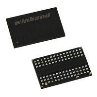
W9751G6IB-25 Winbond Electronics, W9751G6IB-25 Datasheet - Page 27

W9751G6IB-25
Manufacturer Part Number
W9751G6IB-25
Description
IC DDR2-800 SDRAM 512MB 84-WBGA
Manufacturer
Winbond Electronics
Datasheet
1.W9751G6IB-25.pdf
(86 pages)
Specifications of W9751G6IB-25
Format - Memory
RAM
Memory Type
DDR2 SDRAM
Memory Size
512M (32Mx16)
Speed
2.5ns
Interface
Parallel
Voltage - Supply
1.7 V ~ 1.9 V
Operating Temperature
0°C ~ 85°C
Package / Case
84-WBGA
Lead Free Status / RoHS Status
Lead free / RoHS Compliant
Available stocks
Company
Part Number
Manufacturer
Quantity
Price
Company:
Part Number:
W9751G6IB-25
Manufacturer:
WINBOND
Quantity:
15
Company:
Part Number:
W9751G6IB-25
Manufacturer:
WINBOND
Quantity:
1 248
Company:
Part Number:
W9751G6IB-25
Manufacturer:
Winbond Electronics
Quantity:
10 000
Part Number:
W9751G6IB-25
Manufacturer:
WINBOND/华邦
Quantity:
20 000
7.6
The Precharge Command is used to precharge or close a bank that has been activated. The
Precharge Command can be used to precharge each bank independently or all banks simultaneously.
Three address bits A10, BA0 and BA1 are used to define which bank to precharge when the
command is issued.
7.6.1
Minimum Read to Precharge command spacing to the same bank = AL + BL/2 + max(
For the earliest possible precharge, the precharge command may be issued on the rising edge which
is “Additive Latency (AL) + BL/2 + max(
(command) may be issued to the same bank after the RAS precharge time (t
command cannot be issued until t
The minimum Read to Precharge spacing has also to satisfy a minimum analog time from the rising
clock edge that initiates the last 4-bit prefetch of a Read to Precharge command. This time is called
t
command) to Precharge command. For BL = 8 this is the time from AL + 2 clocks after the Read to the
Precharge command. (Example timing waveforms refer to 10.16 to 10.20 Burst read operation
followed by precharge diagram in Chapter 10)
7.6.2
Minimum Write to Precharge Command spacing to the same bank = WL + BL/2 clks + t
For write cycles, a delay must be satisfied from the completion of the last burst write cycle until the
Precharge Command can be issued. This delay is known as a write recovery time (t
from the completion of the burst write to the precharge command. No Precharge command should be
issued prior to the t
followed by precharge diagram in Chapter 10)
7.7
Before a new row in an active bank can be opened, the active bank must be precharged using either
the Precharge command or the Auto-precharge function. When a Read or a Write command is given
to the DDR2 SDRAM, the CAS timing accepts one extra address, column address A10, to allow the
active bank to automatically begin precharge at the earliest possible moment during the burst read or
write cycle. If A10 is LOW when the READ or WRITE command is issued, then normal Read or Write
burst operation is executed and the bank remains active at the completion of the burst sequence. If
A10 is HIGH when the Read or Write command is issued, then the Auto-precharge function is
engaged. During Auto-precharge, a Read command will execute as normal with the exception that the
active bank will begin to precharge on the rising edge which is CAS Latency (CL) clock cycles before
the end of the read burst.
RTP
(Read to Precharge). For BL = 4 this is the time from the actual read (AL after the Read
Precharge operation
Auto-precharge operation
Burst read operation followed by precharge
Burst write operation followed by precharge
HIGH
LOW
LOW
LOW
LOW
A10
WR
Table 4—Bank selection for precharge by address bits
delay. (Example timing waveforms refer to 10.21 to 10.22 Burst write operation
Don’t Care
RAS
HIGH
HIGH
LOW
LOW
BA1
is satisfied.
RTP
, 2) - 2 clocks” after a Read command. A new bank active
- 27 -
Don’t Care
HIGH
HIGH
LOW
LOW
BA0
Publication Release Date: Oct. 23, 2009
RTP
WR
Precharge Bank(s)
W9751G6IB
, 2) - 2 clks
Bank 0 only
Bank 1 only
Bank 2 only
Bank 3 only
All Banks
RP
). A precharge
WR
) referenced
Revision A06


