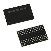
W9751G6IB-25 Winbond Electronics, W9751G6IB-25 Datasheet - Page 65

W9751G6IB-25
Manufacturer Part Number
W9751G6IB-25
Description
IC DDR2-800 SDRAM 512MB 84-WBGA
Manufacturer
Winbond Electronics
Datasheet
1.W9751G6IB-25.pdf
(86 pages)
Specifications of W9751G6IB-25
Format - Memory
RAM
Memory Type
DDR2 SDRAM
Memory Size
512M (32Mx16)
Speed
2.5ns
Interface
Parallel
Voltage - Supply
1.7 V ~ 1.9 V
Operating Temperature
0°C ~ 85°C
Package / Case
84-WBGA
Lead Free Status / RoHS Status
Lead free / RoHS Compliant
Available stocks
Company
Part Number
Manufacturer
Quantity
Price
Company:
Part Number:
W9751G6IB-25
Manufacturer:
WINBOND
Quantity:
15
Company:
Part Number:
W9751G6IB-25
Manufacturer:
WINBOND
Quantity:
1 248
Company:
Part Number:
W9751G6IB-25
Manufacturer:
Winbond Electronics
Quantity:
10 000
Part Number:
W9751G6IB-25
Manufacturer:
WINBOND/华邦
Quantity:
20 000
AC differential input voltage
AC differential cross point input voltage
AC differential cross point output voltage
9.12 AC Input Test Conditions
Notes:
1. Input waveform timing is referenced to the input signal crossing through the VIH/IL(ac) level applied to the device under test.
2. The input signal minimum slew rate is to be maintained over the range from VREF to VIH(ac) min for rising edges and the
3. AC timings are referenced with input waveforms switching from VIL(ac) to VIH(ac) on the positive transitions and VIH(ac) to
9.13 Differential Input/Output AC Logic Levels
(0 ℃ ≤ T
Notes:
1. VID (ac) specifies the input differential voltage |VTR -VCP | required for switching, where VTR is the true input signal (such
2. The typical value of VIX (ac) is expected to be about 0.5 x VDDQ of the transmitting device and VIX (ac) is expected to track
3. The typical value of VOX (ac) is expected to be about 0.5 x VDDQ of the transmitting device and VOX (ac) is expected to
(0 ℃ ≤ T
Input reference voltage
Input signal maximum peak to peak swing
Input signal minimum slew rate
range from VREF to VIL(ac) max for falling edges as shown in the below figure.
VIL(ac) on the negative transitions .
as CLK, LDQS or UDQS) and VCP is the complementary input signal (such as CLK , LDQS or UDQS ). The minimum
value is equal to VIH (ac) - VIL (ac).
variations in VDDQ. VIX (ac) indicates the voltage at which differential input signals must cross.
track variations in VDDQ. VOX (ac) indicates the voltage at which differential output signals must cross.
V
Falling Slew =
SWING(MAX)
CASE
CASE
PARAMETER
△TF
≤ 85 ℃ for 25F/-25/-3, V
≤ 85 ℃ for 25F/-25/-3, V
Figure 28—AC input test signal and Differential signal levels waveform
V
REF -
CONDITION
△TF
V
IL(ac)
max
DD
Rising Slew =
DD
, V
, V
△TR
DDQ
DDQ
V
V
V
= 1.8V ± 0.1V)
V
SYM.
OX (ac)
= 1.8V ± 0.1V)
ID (ac)
IX (ac)
IH(ac)
△TR
min - V
V
V
V
V
V
V
V
DDQ
IL(dc)
IL(ac)
IH(ac)
IH(dc)
REF
SS
V
SLEW
V
REF
max
max
REF
SWING(MAX)
min
min
SYMBOL
0.5 x VDDQ - 0.175
0.5 x VDDQ - 0.125
- 65 -
MIN.
0.5
V
V
TR
CP
Publication Release Date: Oct. 23, 2009
0.5 x VDDQ + 0.175
0.5 x VDDQ + 0.125
0.5 x V
VALUE
VDDQ + 0.6
1.0
1.0
V
V
V
MAX.
DDQ
SSQ
ID
DDQ
W9751G6IB
V
IX
or V
Crossing point
UNIT
V/nS
OX
V
V
UNIT
V
V
V
Revision A06
NOTES
NOTES
2, 3
1
1
1
2
3


