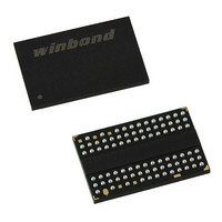
W9751G6IB-25 Winbond Electronics, W9751G6IB-25 Datasheet - Page 18

W9751G6IB-25
Manufacturer Part Number
W9751G6IB-25
Description
IC DDR2-800 SDRAM 512MB 84-WBGA
Manufacturer
Winbond Electronics
Datasheet
1.W9751G6IB-25.pdf
(86 pages)
Specifications of W9751G6IB-25
Format - Memory
RAM
Memory Type
DDR2 SDRAM
Memory Size
512M (32Mx16)
Speed
2.5ns
Interface
Parallel
Voltage - Supply
1.7 V ~ 1.9 V
Operating Temperature
0°C ~ 85°C
Package / Case
84-WBGA
Lead Free Status / RoHS Status
Lead free / RoHS Compliant
Available stocks
Company
Part Number
Manufacturer
Quantity
Price
Company:
Part Number:
W9751G6IB-25
Manufacturer:
WINBOND
Quantity:
15
Company:
Part Number:
W9751G6IB-25
Manufacturer:
WINBOND
Quantity:
1 248
Company:
Part Number:
W9751G6IB-25
Manufacturer:
Winbond Electronics
Quantity:
10 000
Part Number:
W9751G6IB-25
Manufacturer:
WINBOND/华邦
Quantity:
20 000
7.2.4
On-Die Termination (ODT) is a new feature on DDR2 components that allows a DRAM to turn on/off
termination resistance for each DQ, UDQS/ UDQS , LDQS/ LDQS , UDM and LDM signal via the ODT
control pin. UDQS and LDQS are terminated only when enabled in the EMR (1) by address bit A10 =
0. The ODT feature is designed to improve signal integrity of the memory channel by allowing the
DRAM controller to independently turn on/off termination resistance for any or all DRAM devices.
The ODT function can be used for all active and standby modes. ODT is turned off and not supported
in Self Refresh mode. (Example timing waveforms refer to 10.3, 10.4 ODT Timing for
Active/Standby/Power Down Mode and 10.5, 10.6 ODT timing mode switch at entering/exiting power
down mode diagram in Chapter 10)
7.2.5
7.2.5.1
During normal operation the value of the effective termination resistance can be changed with an
EMRS command. The update of the Rtt setting is done between t
must remain HIGH for the entire duration of t
in the following timing diagram.
Switch (sw1, sw2, sw3) is enabled by ODT pin.
Selection among sw1, sw2, and sw3 is determined by “Rtt (nominal)” in EMR (1).
Termination included on all DQs, DM, DQS, DQS pins.
On-Die Termination (ODT)
ODT related timings
MRS command to ODT update delay
Figure 9—Functional Representation of ODT
DRAM
Buffer
Input
V
V
DDQ
SSQ
Rval1
Rval1
sw1
sw1
MOD
window for proper operation. The timings are shown
- 18 -
V
V
DDQ
SSQ
Rval2
Rval2
sw2
sw2
V
V
DDQ
SSQ
Rval3
Rval3
Publication Release Date: Oct. 23, 2009
sw3
sw3
MOD
Input
Pin
,min and t
W9751G6IB
MOD
,max, and CKE
Revision A06


