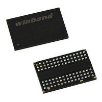
W9751G6IB-25 Winbond Electronics, W9751G6IB-25 Datasheet - Page 24

W9751G6IB-25
Manufacturer Part Number
W9751G6IB-25
Description
IC DDR2-800 SDRAM 512MB 84-WBGA
Manufacturer
Winbond Electronics
Datasheet
1.W9751G6IB-25.pdf
(86 pages)
Specifications of W9751G6IB-25
Format - Memory
RAM
Memory Type
DDR2 SDRAM
Memory Size
512M (32Mx16)
Speed
2.5ns
Interface
Parallel
Voltage - Supply
1.7 V ~ 1.9 V
Operating Temperature
0°C ~ 85°C
Package / Case
84-WBGA
Lead Free Status / RoHS Status
Lead free / RoHS Compliant
Available stocks
Company
Part Number
Manufacturer
Quantity
Price
Company:
Part Number:
W9751G6IB-25
Manufacturer:
WINBOND
Quantity:
15
Company:
Part Number:
W9751G6IB-25
Manufacturer:
WINBOND
Quantity:
1 248
Company:
Part Number:
W9751G6IB-25
Manufacturer:
Winbond Electronics
Quantity:
10 000
Part Number:
W9751G6IB-25
Manufacturer:
WINBOND/华邦
Quantity:
20 000
7.4.2
Burst mode operation is used to provide a constant flow of data to memory locations (write cycle), or
from memory locations (read cycle). The parameters that define how the burst mode will operate are
burst sequence and burst length. The DDR2 SDRAM supports 4 bit and 8 bit burst modes only. For 8
bit burst mode, full interleave address ordering is supported, however, sequential address ordering is
nibble based for ease of implementation. The burst length is programmable and defined by MR A[2:0].
The burst type, either sequential or interleaved, is programmable and defined by MR [A3]. Seamless
burst read or write operations are supported.
Unlike DDR1 devices, interruption of a burst read or writes cycle during BL = 4 mode operation is
prohibited. However in case of BL = 8 mode, interruption of a burst read or write operation is limited to
two cases, reads interrupted by a read, or writes interrupted by a write. (Example timing waveforms
refer to 10.13 and 10.14 Burst read and write interrupt timing diagram in Chapter 10)
DQS/DQS
CLK /CLK
DQS/DQS
CLK/CLK
CMD
CMD
DQ
DQ
Burst mode operation
-1
-1
where AL = 2 and CL = 3, RL = (AL + CL) = 5, WL = (RL - 1) = 4, BL = 4
where AL = 0 and CL = 3, RL = (AL + CL) = 3, WL = (RL - 1) = 2, BL = 4
A-Bank
A-Bank
Figure 14—Example 1: Read followed by a write to the same bank,
Figure 15—Example 2: Read followed by a write to the same bank,
Active
Active
0
0
[AL = 2 and CL = 3, RL = (AL + CL) = 5, WL = (RL - 1) = 4, BL = 4]
AL = 0 and CL = 3, RL = (AL + CL) = 3, WL = (RL - 1) = 2, BL = 4]
≧ t
A-Bank
Read
≧ tRCD
1
1
RCD
AL=2
2
2
AL=0
A-Bank
Read
3
3
RL=AL+CL=5
RL=AL+CL=3
CL=3
4
4
A-Bank
CL=3
Write
- 24 -
5
5
6
6
Dout0
Dout0 Dout1 Dout2 Dout3
Dout1 Dout2 Dout3
A-Bank
Write
WL=RL-1=4
7
7
Publication Release Date: Oct. 23, 2009
WL=RL-1=2
8
8
Din0
Din0
9
9
W9751G6IB
Din1
Din1
10
Din2
Din2
10
Din3
Din3
Revision A06
11
11
12
12


