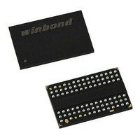
W9751G6IB-25 Winbond Electronics, W9751G6IB-25 Datasheet - Page 23

W9751G6IB-25
Manufacturer Part Number
W9751G6IB-25
Description
IC DDR2-800 SDRAM 512MB 84-WBGA
Manufacturer
Winbond Electronics
Datasheet
1.W9751G6IB-25.pdf
(86 pages)
Specifications of W9751G6IB-25
Format - Memory
RAM
Memory Type
DDR2 SDRAM
Memory Size
512M (32Mx16)
Speed
2.5ns
Interface
Parallel
Voltage - Supply
1.7 V ~ 1.9 V
Operating Temperature
0°C ~ 85°C
Package / Case
84-WBGA
Lead Free Status / RoHS Status
Lead free / RoHS Compliant
Available stocks
Company
Part Number
Manufacturer
Quantity
Price
Company:
Part Number:
W9751G6IB-25
Manufacturer:
WINBOND
Quantity:
15
Company:
Part Number:
W9751G6IB-25
Manufacturer:
WINBOND
Quantity:
1 248
Company:
Part Number:
W9751G6IB-25
Manufacturer:
Winbond Electronics
Quantity:
10 000
Part Number:
W9751G6IB-25
Manufacturer:
WINBOND/华邦
Quantity:
20 000
W9751G6IB
7.3.10 No-Operation Command
( CS = "L", RAS = "H", CAS = "H", WE = "H", CKE, BA0, BA1, A0 to A12 = Don’t Care)
The No-Operation command simply performs no operation (same command as Device Deselect).
7.3.11 Device Deselect Command
( CS = "H", RAS , CAS , WE , CKE, BA0, BA1, A0 to A12 = Don’t Care)
The Device Deselect command disables the command decoder so that the RAS , CAS , WE and
Address inputs are ignored. This command is similar to the No-Operation command.
7.4
Read and Write access modes
The DDR2 SDRAM provides a fast column access operation. A single Read or Write Command will
initiate a serial read or write operation on successive clock cycles. The boundary of the burst cycle is
strictly restricted to specific segments of the page length.
*
The 8 Mbit x 16 I/O x 4 Bank chip has a page length of 1024 bits (defined by CA0 to CA9)
. The page
length of 1024 is divided into 256 or 128 uniquely addressable boundary segments depending on
burst length, 256 for 4 bit burst, 128 for 8 bit burst respectively. A 4-bit or 8-bit burst operation will
occur entirely within one of the 256 or 128 groups beginning with the column address supplied to the
device during the Read or Write Command (CA0 to CA9). The second, third and fourth access will
also occur within this group segment. However, the burst order is a function of the starting address,
and the burst sequence.
A new burst access must not interrupt the previous 4 bit burst operation in case of BL = 4 setting.
However, in case of BL = 8 setting, two cases of interrupt by a new burst access are allowed, one
reads interrupted by a read, the other writes interrupted by a write with 4 bit burst boundary
respectively. The minimum CAS to CAS delay is defined by t
, and is a minimum of 2 clocks for
CCD
read or write cycles.
Note: Page length is a function of I/O organization and column addressing
8M bits × 16 organization (CA0 to CA9); Page Length = 1024 bits
7.4.1
Posted
CAS
Posted CAS operation is supported to make command and data bus efficient for sustainable
bandwidths in DDR2 SDRAM. In this operation, the DDR2 SDRAM allows a CAS read or write
command to be issued immediately after the RAS bank activate command (or any time during the
RAS - CAS -delay time, t
, period). The command is held for the time of the Additive Latency (AL)
RCD
before it is issued inside the device. The Read Latency (RL) is controlled by the sum of AL and the
CAS Latency (CL). Therefore if a user chooses to issue a Read/Write command before the t
,
RCDmin
then AL (greater than 0) must be written into the EMR (1). The Write Latency (WL) is always defined
as RL -1 (Read Latency -1) where Read Latency is defined as the sum of Additive Latency plus CAS
Latency (RL = AL + CL). Read or Write operations using AL allow seamless bursts. (Example timing
waveforms refer to 10.11 and 10.12 seamless burst read/write operation diagram in Chapter 10)
7.4.1.1
Examples of posted
operation
CAS
Examples of a read followed by a write to the same bank where AL = 2 and where AL = 0 are shown
in Figures 14 and 15, respectively.
Publication Release Date: Oct. 23, 2009
- 23 -
Revision A06


