W9751G6IB-25 Winbond Electronics, W9751G6IB-25 Datasheet - Page 16
W9751G6IB-25
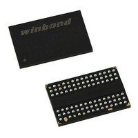
Manufacturer Part Number
W9751G6IB-25
Description
IC DDR2-800 SDRAM 512MB 84-WBGA
Manufacturer
Winbond Electronics
Datasheet
1.W9751G6IB-25.pdf
(86 pages)
Specifications of W9751G6IB-25
Format - Memory
RAM
Memory Type
DDR2 SDRAM
Memory Size
512M (32Mx16)
Speed
2.5ns
Interface
Parallel
Voltage - Supply
1.7 V ~ 1.9 V
Operating Temperature
0°C ~ 85°C
Package / Case
84-WBGA
Lead Free Status / RoHS Status
Lead free / RoHS Compliant
Available stocks
Company
Part Number
Manufacturer
Quantity
Price
Company:

Part Number:
W9751G6IB-25
Manufacturer:
WINBOND
Quantity:
15
Company:
Part Number:
W9751G6IB-25
Manufacturer:
WINBOND
Quantity:
1 248
Company:
Part Number:
W9751G6IB-25
Manufacturer:
Winbond Electronics
Quantity:
10 000
Part Number:
W9751G6IB-25
Manufacturer:
WINBOND/华邦
Quantity:
20 000


7.2.3.1
OCD impedance adjustment can be done using the following EMRS mode. In drive mode all outputs
are driven out by DDR2 SDRAM. In Drive (1) mode, all DQ, DQS signals are driven HIGH and all
signals are driven HIGH. In adjust mode, BL = 4 of operation code data must be used. In case of OCD
calibration default, output driver characteristics have a nominal impedance value of 18 Ohms during
nominal temperature and voltage conditions. OCD applies only to normal full strength output drive
setting defined by EMR (1) and if reduced strength is set, OCD default driver characteristics are not
applicable. When OCD calibration adjust mode is used, OCD default output driver characteristics are
not applicable. After OCD calibration is completed or driver strength is set to default, subsequent
EMRS commands not intended to adjust OCD characteristics must specify A[9:7] as ’000’ in order to
maintain the default or calibrated value.
7.2.3.2
To adjust output driver impedance, controllers must issue the ADJUST EMRS command along with a
4 bit burst code to DDR2 SDRAM as in table 2. For this operation, Burst Length has to be set to BL =
4 via MRS command before activating OCD and controllers must drive the burst code to all DQs at the
same time. D
output impedance is adjusted for all DDR2 SDRAM DQs simultaneously and after OCD calibration, all
DQs and DQS’s of a given DDR2 SDRAM will be adjusted to the same driver strength setting. The
maximum step count for adjustment is 16 and when the limit is reached, further increment or
decrement code has no effect. The default setting may be any step within the 16 step range. When
Adjust mode command is issued, AL from previously set value must be applied.
DQS signals are driven LOW. In Drive (0) mode, all DQ, DQS signals are driven LOW and all DQS
D
4 bit burst code inputs to all DQs
0
0
0
0
1
0
0
1
1
T0
A9
0
0
0
1
1
Extended Mode Register for OCD Impedance Adjustment
OCD Impedance Adjust
Other Combinations
D
T0
0
0
0
1
0
1
1
0
0
T1
A8
in table 2 means all DQ bits at bit time 0, D
0
0
1
0
1
D
0
0
1
0
0
0
1
0
1
T2
A7
0
1
0
0
1
Table 2—OCD Adjust Mode Program
Table 1—OCD Drive Mode Program
D
0
1
0
0
0
1
0
1
0
T3
Operation
OCD calibration mode exit
Drive (1) DQ, DQS HIGH and DQS LOW
Drive (0) DQ, DQS LOW and DQS HIGH
Adjust mode
OCD calibration default
NOP (No operation)
Increase by 1 step
Decrease by 1 step
NOP
NOP
Increase by 1 step
Decrease by 1 step
Increase by 1 step
Decrease by 1 step
Pull-up driver strength
- 16 -
T1
at bit time 1, and so forth. The driver
Publication Release Date: Oct. 23, 2009
Operation
Reserved
NOP (No operation)
NOP
NOP
Increase by 1 step
Decrease by 1 step
Increase by 1 step
Increase by 1 step
Decrease by 1 step
Decrease by 1 step
Pull-down driver strength
W9751G6IB
Revision A06
Related parts for W9751G6IB-25
Image
Part Number
Description
Manufacturer
Datasheet
Request
R

Part Number:
Description:
Winbond H/w Monitoring Ic
Manufacturer:
Winbond Electronics Corp America
Datasheet:
Part Number:
Description:
Winbond Lpc I/o
Manufacturer:
Winbond Electronics Corp America
Datasheet:
Part Number:
Description:
Winbond Smbus Gpi/o
Manufacturer:
Winbond Electronics Corp America
Datasheet:
Part Number:
Description:
Winbond I/o
Manufacturer:
Winbond Electronics Corp America
Datasheet:
Part Number:
Description:
Winbond Clock Generator For Intel P4 Springdale Series Chipset
Manufacturer:
Winbond Electronics Corp America
Datasheet:
Part Number:
Description:
Winbond Clock Generator For Intel P4 Springdale Series Chipset
Manufacturer:
Winbond Electronics Corp America
Datasheet:
Part Number:
Description:
Winbond Clock Generator For Intel P4 Springdale Series Chipset P4 Springdale Series Chipset
Manufacturer:
Winbond Electronics Corp America
Datasheet:
Part Number:
Description:
Winbond Clock Generator For Intel P4 845 Series Chipset
Manufacturer:
Winbond Electronics Corp America
Datasheet:
Part Number:
Description:
Winbond Clock Generator For Via P4/kt Series Chipset
Manufacturer:
Winbond Electronics Corp America
Datasheet:
Part Number:
Description:
Winbond Clock Generator For Intel 915/925 Chipsets
Manufacturer:
Winbond Electronics Corp America
Datasheet:
Part Number:
Description:
Winbond H/w Monitoring Ic
Manufacturer:
Winbond Electronics Corp America
Datasheet:
Part Number:
Description:
Winbond Lpc I/o
Manufacturer:
Winbond Electronics Corp America
Datasheet:
Part Number:
Description:
Winbond Smbus Gpi/o
Manufacturer:
Winbond Electronics Corp America
Datasheet:
Part Number:
Description:
Winbond I/o
Manufacturer:
Winbond Electronics Corp America
Datasheet:

Part Number:
Description:
IC SPI FLASH 4MBIT 8SOIC
Manufacturer:
Winbond Electronics
Datasheet: