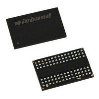
W9751G6IB-25 Winbond Electronics, W9751G6IB-25 Datasheet - Page 20

W9751G6IB-25
Manufacturer Part Number
W9751G6IB-25
Description
IC DDR2-800 SDRAM 512MB 84-WBGA
Manufacturer
Winbond Electronics
Datasheet
1.W9751G6IB-25.pdf
(86 pages)
Specifications of W9751G6IB-25
Format - Memory
RAM
Memory Type
DDR2 SDRAM
Memory Size
512M (32Mx16)
Speed
2.5ns
Interface
Parallel
Voltage - Supply
1.7 V ~ 1.9 V
Operating Temperature
0°C ~ 85°C
Package / Case
84-WBGA
Lead Free Status / RoHS Status
Lead free / RoHS Compliant
Available stocks
Company
Part Number
Manufacturer
Quantity
Price
Company:
Part Number:
W9751G6IB-25
Manufacturer:
WINBOND
Quantity:
15
Company:
Part Number:
W9751G6IB-25
Manufacturer:
WINBOND
Quantity:
1 248
Company:
Part Number:
W9751G6IB-25
Manufacturer:
Winbond Electronics
Quantity:
10 000
Part Number:
W9751G6IB-25
Manufacturer:
WINBOND/华邦
Quantity:
20 000
7.3
7.3.1
( CS = "L", RAS = "L", CAS = "H", WE = "H", BA0, BA1 = Bank, A0 to A12 be row address)
The Bank Activate command must be applied before any Read or Write operation can be executed.
Immediately after the bank active command, the DDR2 SDRAM can accept a read or write command
on the following clock cycle. If a Read/Write command is issued to a bank that has not satisfied the
t
Read/Write command is internally issued to the device. The additive latency value must be chosen to
assure t
activated it must be precharged before another Bank Activate command can be applied to the same
bank. The bank active and precharge times are defined as t
time interval between successive Bank Activate commands to the same bank is determined by the
RAS cycle time of the device (t
t
7.3.2
( CS = "L", RAS = "H", CAS = "L", WE = "H", BA0, BA1 = Bank, A10 = "L", A0 to A9 = Column
Address)
The READ command is used to initiate a burst read access to an active row. The value on BA0, BA1
inputs selects the bank, and the A0 to A9 address inputs determine the starting column address. The
address input A10 determines whether or not Auto-precharge is used. If Auto-precharge is selected,
the row being accessed will be precharged at the end of the READ burst; if Auto-precharge is not
selected, the row will remain open for subsequent accesses.
RCDmin
RRD
.
Figure 12—Bank activate command cycle: t
Command Function
Bank Activate Command
RCDmin
Read Command
specification, then additive latency must be programmed into the device to delay when the
is satisfied. Additive latencies of 0, 1, 2, 3 and 4 are supported. Once a bank has been
RC
). The minimum time interval between Bank Activate commands is
- 20 -
RCD
= 3, AL = 2, t
RAS
Publication Release Date: Oct. 23, 2009
and t
RP
RP
= 3, t
, respectively. The minimum
RRD
W9751G6IB
= 2, t
CCD
Revision A06
= 2


