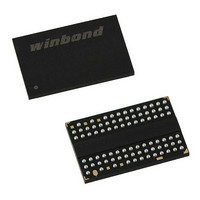
W9751G6IB-25 Winbond Electronics, W9751G6IB-25 Datasheet - Page 32

W9751G6IB-25
Manufacturer Part Number
W9751G6IB-25
Description
IC DDR2-800 SDRAM 512MB 84-WBGA
Manufacturer
Winbond Electronics
Datasheet
1.W9751G6IB-25.pdf
(86 pages)
Specifications of W9751G6IB-25
Format - Memory
RAM
Memory Type
DDR2 SDRAM
Memory Size
512M (32Mx16)
Speed
2.5ns
Interface
Parallel
Voltage - Supply
1.7 V ~ 1.9 V
Operating Temperature
0°C ~ 85°C
Package / Case
84-WBGA
Lead Free Status / RoHS Status
Lead free / RoHS Compliant
Available stocks
Company
Part Number
Manufacturer
Quantity
Price
Company:
Part Number:
W9751G6IB-25
Manufacturer:
WINBOND
Quantity:
15
Company:
Part Number:
W9751G6IB-25
Manufacturer:
WINBOND
Quantity:
1 248
Company:
Part Number:
W9751G6IB-25
Manufacturer:
Winbond Electronics
Quantity:
10 000
Part Number:
W9751G6IB-25
Manufacturer:
WINBOND/华邦
Quantity:
20 000
8.2
Notes:
1. CKE (N) is the logic state of CKE at clock edge N; CKE (N–1) was the state of CKE at the previous clock edge.
2. Current state is the state of the DDR2 SDRAM immediately prior to clock edge N.
3. COMMAND (N) is the command registered at clock edge N, and ACTION (N) is a result of COMMAND (N).
4. All states and sequences not shown are illegal or reserved unless explicitly described elsewhere in this document.
5. On Self Refresh Exit DESELECT or NOP commands must be issued on every clock edge occurring during the t
6. Self Refresh mode can only be entered from the All Banks Idle state.
7. Must be a legal command as defined in the Command Truth Table.
8. Valid commands for Power Down Entry and Exit are NOP and DESELECT only.
9. Valid commands for Self Refresh Exit are NOP and DESELECT only.
10. Power Down and Self Refresh can not be entered while Read or Write operations, (Extended) Mode Register Set
11. tCKEmin of 3 clocks means CKE must be registered on three consecutive positive clock edges. CKE must remain at the
12. The state of ODT does not affect the states described in this table. The ODT function is not available during Self Refresh.
13. The Power Down does not perform any refresh operations. The duration of Power Down Mode is therefore limited by the
14. CKE must be maintained HIGH while the SDRAM is in OCD calibration mode.
15. ”X” means “don’t care (including floating around V
16. V
8.3
Note:
1. Used to mask write data, provided coincident with the corresponding data.
Bank(s) Active
All Banks Idle
Power Down
Self Refresh
CURRENT
Read commands may be issued only after t
operations or Precharge operations are in progress. See section 7.9 "Power Down Mode" and section 7.3.7/7.3.8 "Self
Refresh Entry/Exit Command" for a detailed list of restrictions.
valid input level the entire time it takes to achieve the 3 clocks of registration. Thus, after any CKE transition, CKE may not
transition from its valid level during the time period of t
See section 7.2.4.
refresh requirements outlined in section 7.9.
high or low in Power Down if the ODT function is enabled (Bit A2 or A6 set to “1” in EMR (1)).
STATE
REF
FUNCTION
Write enable
Write inhibit
Clock Enable (CKE) Truth Table for Synchronous Transitions
Data Mask (DM) Truth Table
must be maintained during Self Refresh operation.
2
Previous Cycle
(N-1)
H
H
H
H
L
L
L
L
CKE
1
Current Cycle
DM
H
L
XSRD
(N)
H
H
H
L
L
L
L
L
(200 clocks) is satisfied.
REF
1
)” in Self Refresh and Power Down. However ODT must be driven
IS
+ 2 x t
RAS , CAS , WE , CS
- 32 -
DESELECT or NOP
DESELECT or NOP
DESELECT or NOP
DESELECT or NOP
COMMAND (N)
CK
REFRESH
Refer to the Command Truth Table
+ t
X
X
IH
.
3
Publication Release Date: Oct. 23, 2009
DQS
Valid
Precharge Power Down
X
Maintain Power Down
Maintain Power Down
Active Power Down
Self Refresh Entry
Power Down Exit
Self Refresh Exit
ACTION (N)
Entry
Entry
W9751G6IB
3
Revision A06
XSNR
4, 8, 10, 11,
4, 8, 10, 11,
4, 8, 11, 13
6, 9, 11, 13
11, 13, 15
11, 15, 16
4, 5, 9, 16
NOTE
NOTES
1
1
13
13
7
period.


