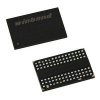
W9751G6IB-25 Winbond Electronics, W9751G6IB-25 Datasheet - Page 53

W9751G6IB-25
Manufacturer Part Number
W9751G6IB-25
Description
IC DDR2-800 SDRAM 512MB 84-WBGA
Manufacturer
Winbond Electronics
Datasheet
1.W9751G6IB-25.pdf
(86 pages)
Specifications of W9751G6IB-25
Format - Memory
RAM
Memory Type
DDR2 SDRAM
Memory Size
512M (32Mx16)
Speed
2.5ns
Interface
Parallel
Voltage - Supply
1.7 V ~ 1.9 V
Operating Temperature
0°C ~ 85°C
Package / Case
84-WBGA
Lead Free Status / RoHS Status
Lead free / RoHS Compliant
Available stocks
Company
Part Number
Manufacturer
Quantity
Price
Company:
Part Number:
W9751G6IB-25
Manufacturer:
WINBOND
Quantity:
15
Company:
Part Number:
W9751G6IB-25
Manufacturer:
WINBOND
Quantity:
1 248
Company:
Part Number:
W9751G6IB-25
Manufacturer:
Winbond Electronics
Quantity:
10 000
Part Number:
W9751G6IB-25
Manufacturer:
WINBOND/华邦
Quantity:
20 000
31. These parameters are specified per their average values, however it is understood that the following relationship between
Example: For DDR2-667, tCH(abs),min = ( 0.48 x 3000 pS ) - 125 pS = 1315 pS
32. tHP is the minimum of the absolute half period of the actual input clock. tHP is an input parameter but not an input
33. tQHS accounts for:
34. tQH = tHP – tQHS, where:
35. When the device is operated with input clock jitter, this parameter needs to be derated by the actual tERR(6-10per) of the
Absolute clock period
Absolute clock HIGH pulse width
Absolute clock LOW pulse width
the average timing and the absolute instantaneous timing holds at all times. (Min and max of SPEC values are to be used
for calculations in the table below.)
specification parameter. It is used in conjunction with tQHS to derive the DRAM output timing tQH. The value to be used for
tQH calculation is determined by the following equation;
input clock. (output deratings are relative to the SDRAM input clock.)
PARAMETER
tHP = Min ( tCH(abs), tCL(abs) ),
where,
tCH(abs) is the minimum of the actual instantaneous clock HIGH time;
tCL(abs) is the minimum of the actual instantaneous clock LOW time;
1) The pulse duration distortion of on-chip clock circuits, which represents how well the actual tHP at the input is
transferred to the output; and
2) The worst case push-out of DQS on one transition followed by the worst case pull-in of DQ on the next transition,
both of which are independent of each other, due to data pin skew, output pattern effects, and p-channel to n-
channel variation of the output drivers
tHP is the minimum of the absolute half period of the actual input clock; and
tQHS is the specification value under the max column.
{The less half-pulse width distortion present, the larger the tQH value is; and the larger the valid data eye will be.}
Examples:
1) If the system provides tHP of 1315 pS into a DDR2-667 SDRAM, the DRAM provides tQH of 975 pS minimum.
2) If the system provides tHP of 1420 pS into a DDR2-667 SDRAM, the DRAM provides tQH of 1080 pS minimum.
Example:
If the measured jitter into a DDR2-667 SDRAM has tERR(6-10per),min = - 272 pS and tERR(6-10per),max = + 293
pS, then tDQSCK,min(derated) = tDQSCK,min - tERR(6-10per),max = - 400 pS - 293 pS = - 693 pS and
tDQSCK,max(derated) = tDQSCK,max - tERR(6-10per),min = 400 pS + 272 pS = + 672 pS.
Similarly, tLZ(DQ) for DDR2-667 derates to tLZ(DQ),min(derated) = - 900 pS - 293 pS = - 1193 pS and
tLZ(DQ),max(derated) = 450 pS + 272 pS = + 722 pS. (Caution on the min/max usage!)
SYMBOL
tCK(abs)
tCH(abs)
tCL(abs)
tCH(avg),min x tCK(avg),min +
tCL(avg),min x tCK(avg),min +
tCK(avg),min + tJIT(per),min
tJIT(duty),min
tJIT(duty),min
- 53 -
MIN
Publication Release Date: Oct. 23, 2009
tCH(avg),max x tCK(avg),max +
tCL(avg),max x tCK(avg),max +
tCK(avg),max + tJIT(per),max
tJIT(duty),max
tJIT(duty),max
MAX
W9751G6IB
Revision A06
UNIT
pS
pS
pS


