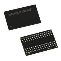
W9751G6IB-25 Winbond Electronics, W9751G6IB-25 Datasheet - Page 39

W9751G6IB-25
Manufacturer Part Number
W9751G6IB-25
Description
IC DDR2-800 SDRAM 512MB 84-WBGA
Manufacturer
Winbond Electronics
Datasheet
1.W9751G6IB-25.pdf
(86 pages)
Specifications of W9751G6IB-25
Format - Memory
RAM
Memory Type
DDR2 SDRAM
Memory Size
512M (32Mx16)
Speed
2.5ns
Interface
Parallel
Voltage - Supply
1.7 V ~ 1.9 V
Operating Temperature
0°C ~ 85°C
Package / Case
84-WBGA
Lead Free Status / RoHS Status
Lead free / RoHS Compliant
Available stocks
Company
Part Number
Manufacturer
Quantity
Price
Company:
Part Number:
W9751G6IB-25
Manufacturer:
WINBOND
Quantity:
15
Company:
Part Number:
W9751G6IB-25
Manufacturer:
WINBOND
Quantity:
1 248
Company:
Part Number:
W9751G6IB-25
Manufacturer:
Winbond Electronics
Quantity:
10 000
Part Number:
W9751G6IB-25
Manufacturer:
WINBOND/华邦
Quantity:
20 000
9.7
9.8
Notes:
1. All other pins not under test = 0 V.
2. DQ, LDQS, LDQS , UDQS, UDQS are disabled and ODT is turned off.
3. V
4. V
5. The values of I
0.28V.
capability to ensure V
I
DDQ
DDQ
I
SYM.
SYM.
C
OH(dc)
OL(dc)
C
C
V
V
C
C
I
DCK
C
I
DIO
OL
OH
Capacitance
CK
Leakage and Output Buffer Characteristics
IL
OL
DI
IO
I
= 1.7 V; V
= 1.7 V; V
OH(dc)
Input Capacitance , CLK and
Input Capacitance delta , CLK and
input Capacitance, all other input-only pins
Input Capacitance delta, all other input-only pins
Input/output Capacitance, DQ, LDM, UDM, LDQS,
Input/output Capacitance delta, DQ, LDM, UDM,
LDQS,
Input Leakage Current
(0V≦V
Output Leakage Current
(Output disabled, 0V≦V
Minimum Required Output Pull-up
Maximum Required Output Pull-down
Output Minimum Source DC Current
Output Minimum Sink DC Current
LDQS
OUT
OUT
= 1.42 V. (V
= 0.28V. V
IH
and
min plus a noise margin and V
IN
, UDQS,
LDQS
≦V
IOL(dc)
PARAMETER
DD
OUT
, UDQS,
OUT
are based on the conditions given in Notes 3 and 4. They are used to test drive current
)
UDQS
PARAMETER
/I
OL
- V
must be less than 21 Ω for values of V
DDQ
OUT
UDQS
)/I
OH
≦V
CLK
must be less than 21 Ω for values of V
DDQ
IL
max minus a noise margin are delivered to an SSTL_18 receiver.
CLK
)
- 39 -
V
TT
MIN.
-13.4
13.4
+ 0.603
-2
-5
−
OUT
Publication Release Date: Oct. 23, 2009
V
MIN.
TT
1.0
1.0
2.5
MAX.
−
−
−
between 0 V and 0.28V.
- 0.603
2
5
−
−
−
OUT
between V
W9751G6IB
UNIT
MAX.
mA
mA
µA
µA
0.25
0.25
V
V
2.0
2.0
3.5
0.5
DDQ
and V
Revision A06
NOTES
3, 5
4, 5
UNIT
1
2
DDQ
pF
pF
pF
pF
pF
pF
-


