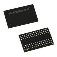
W9751G6IB-25 Winbond Electronics, W9751G6IB-25 Datasheet - Page 9

W9751G6IB-25
Manufacturer Part Number
W9751G6IB-25
Description
IC DDR2-800 SDRAM 512MB 84-WBGA
Manufacturer
Winbond Electronics
Datasheet
1.W9751G6IB-25.pdf
(86 pages)
Specifications of W9751G6IB-25
Format - Memory
RAM
Memory Type
DDR2 SDRAM
Memory Size
512M (32Mx16)
Speed
2.5ns
Interface
Parallel
Voltage - Supply
1.7 V ~ 1.9 V
Operating Temperature
0°C ~ 85°C
Package / Case
84-WBGA
Lead Free Status / RoHS Status
Lead free / RoHS Compliant
Available stocks
Company
Part Number
Manufacturer
Quantity
Price
Company:
Part Number:
W9751G6IB-25
Manufacturer:
WINBOND
Quantity:
15
Company:
Part Number:
W9751G6IB-25
Manufacturer:
WINBOND
Quantity:
1 248
Company:
Part Number:
W9751G6IB-25
Manufacturer:
Winbond Electronics
Quantity:
10 000
Part Number:
W9751G6IB-25
Manufacturer:
WINBOND/华邦
Quantity:
20 000
7. FUNCTIONAL DESCRIPTION
7.1
DDR2 SDRAMs must be powered up and initialized in a predefined manner. Operational procedures
other than those specified may result in undefined operation. The following sequence is required for
Power-up and Initialization.
1. Apply power and attempt to maintain CKE below 0.2 × V
2. Start Clock and maintain stable condition for 200 µS (min.).
3. After stable power and clock (CLK, CLK ), apply NOP or Deselect and take CKE HIGH.
4. Wait minimum of 400 nS then issue precharge all command. NOP or Deselect applied during 400
5. Issue an EMRS command to EMR (2). (To issue EMRS command to EMR (2), provide LOW to
6. Issue an EMRS command to EMR (3). (To issue EMRS command to EMR (3), provide HIGH to
7. Issue EMRS to enable DLL. (To issue DLL Enable command, provide LOW to A0, HIGH to BA0
8. Issue a Mode Register Set command for DLL reset. (To issue DLL Reset command, provide HIGH
9. Issue a precharge all command.
10. Issue 2 or more Auto Refresh commands.
11. Issue a MRS command with LOW to A8 to initialize device operation. (i.e. to program operating
12. At least 200 clocks after step 8, execute OCD Calibration (Off Chip Driver impedance adjustment).
13. The DDR2 SDRAM is now ready for normal operation.
A. The V
B. Voltage levels at I/Os and outputs must be less than V
inputs may be undefined.) Either one of the following sequence is required for Power-up.
nS period.
BA0, HIGH to BA1.)
BA0 and BA1.)
and LOW to BA1. And A9=A8=A7=LOW must be used when issuing this command.)
to A8 and LOW to BA0 and BA1.)
parameters without resetting the DLL.)
If OCD calibration is not used, EMRS to EMR (1) to set OCD Calibration Default
(A9=A8=A7=HIGH) followed by EMRS to EMR (1) to exit OCD Calibration Mode
(A9=A8=A7=LOW) must be issued with other operating parameters of EMR(1).
Power-up and Initialization Sequence
mV to V
DRAM latch-up. During the ramping of the supply voltages, V
maintained and is applicable to both AC and DC levels until the ramping of the supply voltages
is complete.
V
V
V
V
Apply V
Apply V
V
V
DD
TT
REF
DDQ
REF
DDQ
DD
, V
is limited to 0.95V max
DD
*2
*2
voltage ramp time must be no greater than 200 mS from when V
≧ V
≧ V
DDL
tracks V
tracks V
DD
DDQ
min; and during the V
/V
and V
REF
REF
*4
DDL
before or at the same time as V
DDQ
DDQ
must be met at all times
must be met at all times.
*3
DDQ
before or at the same time as V
/2
/2
are driven from a single power converter output
DD
voltage ramp, |V
- 9 -
TT
DD
DDQ
DDQ
-V
DDQ
DDQ
Publication Release Date: Oct. 23, 2009
and ODT
during voltage ramp time to avoid
| ≦ 0.3 volts.
DD
≧ V
*1
at a LOW state (all other
DDL
W9751G6IB
DD
≧ V
ramps from 300
DDQ
Revision A06
must be


