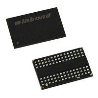
W9751G6IB-25 Winbond Electronics, W9751G6IB-25 Datasheet - Page 30

W9751G6IB-25
Manufacturer Part Number
W9751G6IB-25
Description
IC DDR2-800 SDRAM 512MB 84-WBGA
Manufacturer
Winbond Electronics
Datasheet
1.W9751G6IB-25.pdf
(86 pages)
Specifications of W9751G6IB-25
Format - Memory
RAM
Memory Type
DDR2 SDRAM
Memory Size
512M (32Mx16)
Speed
2.5ns
Interface
Parallel
Voltage - Supply
1.7 V ~ 1.9 V
Operating Temperature
0°C ~ 85°C
Package / Case
84-WBGA
Lead Free Status / RoHS Status
Lead free / RoHS Compliant
Available stocks
Company
Part Number
Manufacturer
Quantity
Price
Company:
Part Number:
W9751G6IB-25
Manufacturer:
WINBOND
Quantity:
15
Company:
Part Number:
W9751G6IB-25
Manufacturer:
WINBOND
Quantity:
1 248
Company:
Part Number:
W9751G6IB-25
Manufacturer:
Winbond Electronics
Quantity:
10 000
Part Number:
W9751G6IB-25
Manufacturer:
WINBOND/华邦
Quantity:
20 000
7.9.1
Two types of Power Down Mode can be performed on the device: Precharge Power Down Mode and
Active Power Down Mode.
If power down occurs when all banks are idle, this mode is referred to as Precharge Power Down; if
power down occurs when there is a row active in any bank, this mode is referred to as Active Power
Down. Entering power down deactivates the input and output buffers, excluding CLK, CLK , ODT and
CKE. Also the DLL is disabled upon entering Precharge Power Down or slow exit Active Power Down,
but the DLL is kept enabled during fast exit Active Power Down.
In power down mode, CKE LOW and a stable clock signal must be maintained at the inputs of the
DDR2 SDRAM, and ODT should be in a valid state but all other input signals are “Don’t Care”. CKE
LOW must be maintained until t
the refresh requirements of the device, which allows a maximum of 9 x
REF is utilized immediately before entering power down. (Example timing waveforms refer to 10.30 to
10.31 Active and Precharged Power Down Mode Entry and Exit diagram in Chapter 10)
7.9.2
The power-down state is synchronously exited when CKE is registered HIGH (along with a NOP or
Deselect command). CKE high must be maintained until t
command can be applied with power-down exit latency, t
Power-down exit latency is defined at AC Characteristics table of this data sheet.
7.10 Input clock frequency change during precharge power down
DDR2 SDRAM input clock frequency can be changed under following condition:
DDR2 SDRAM is in precharged power down mode. ODT must be turned off and CKE must be at logic
LOW level. A minimum of 2 clocks must be waited after CKE goes LOW before clock frequency may
change. SDRAM input clock frequency is allowed to change only within minimum and maximum
operating frequency specified for the particular speed grade. During input clock frequency change,
ODT and CKE must be held at stable LOW levels.
Once input clock frequency is changed, stable new clocks must be provided to DRAM before
precharge power down may be exited and DLL must be RESET via MRS command after precharge
power down exit. Depending on new clock frequency an additional MRS or EMRS command may
need to be issued to appropriately set the WR, CL etc…
During DLL re-lock period, ODT must remain off. After the DLL lock time, the DRAM is ready to
operate with new clock frequency. (Example timing waveform refer to 10.32 Clock frequency change
in precharge Power Down mode diagram in Chapter 10)
Power Down Entry
Power Down Exit
CKE
has been satisfied. Maximum power down duration is limited by
- 30 -
XP
CKE
, t
XARD
has been satisfied. A valid, executable
Publication Release Date: Oct. 23, 2009
, or t
XARDS
tREFI
, after CKE goes HIGH.
if maximum posting of
W9751G6IB
Revision A06


