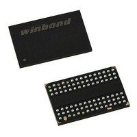
W9751G6IB-25 Winbond Electronics, W9751G6IB-25 Datasheet - Page 60

W9751G6IB-25
Manufacturer Part Number
W9751G6IB-25
Description
IC DDR2-800 SDRAM 512MB 84-WBGA
Manufacturer
Winbond Electronics
Datasheet
1.W9751G6IB-25.pdf
(86 pages)
Specifications of W9751G6IB-25
Format - Memory
RAM
Memory Type
DDR2 SDRAM
Memory Size
512M (32Mx16)
Speed
2.5ns
Interface
Parallel
Voltage - Supply
1.7 V ~ 1.9 V
Operating Temperature
0°C ~ 85°C
Package / Case
84-WBGA
Lead Free Status / RoHS Status
Lead free / RoHS Compliant
Available stocks
Company
Part Number
Manufacturer
Quantity
Price
Company:
Part Number:
W9751G6IB-25
Manufacturer:
WINBOND
Quantity:
15
Company:
Part Number:
W9751G6IB-25
Manufacturer:
WINBOND
Quantity:
1 248
Company:
Part Number:
W9751G6IB-25
Manufacturer:
Winbond Electronics
Quantity:
10 000
Part Number:
W9751G6IB-25
Manufacturer:
WINBOND/华邦
Quantity:
20 000
44. Data setup and hold time derating.
For all input signals the total tDS (setup time) and tDH (hold time) required is calculated by adding the data sheet tDS(base) and
tDH(base) value to the ΔtDS and ΔtDH derating value respectively. Example: tDS (total setup time) = tDS(base) + ΔtDS.
Setup (tDS) nominal slew rate for a rising signal is defined as the slew rate between the last crossing of VREF(dc) and the first
crossing of VIH(ac)min. Setup (tDS) nominal slew rate for a falling signal is defined as the slew rate between the last crossing of
VREF(dc) and the first crossing of VIL(ac)max. If the actual signal is always earlier than the nominal slew rate line between
shaded ‘VREF(dc) to AC region’, use nominal slew rate for derating value. See Figure 24 Illustration of nominal slew rate for
tDS (differential DQS, DQS ).
If the actual signal is later than the nominal slew rate line anywhere between shaded ‘VREF(dc) to AC region’, the slew rate of a
tangent line to the actual signal from the AC level to DC level is used for derating value. See Figure 25 Illustration of tangent line
for tDS (differential DQS, DQS ).
Hold (tDH) nominal slew rate for a rising signal is defined as the slew rate between the last crossing of VIL(dc)max and the first
crossing of VREF(dc). Hold (tDH) nominal slew rate for a falling signal is defined as the slew rate between the last crossing of
VIH(dc)min and the first crossing of VREF(dc). If the actual signal is always later than the nominal slew rate line between
shaded ‘DC level to VREF(dc) region’, use nominal slew rate for derating value. See Figure 26 Illustration of nominal slew rate
for tDH (differential DQS, DQS ).
If the actual signal is earlier than the nominal slew rate line anywhere between shaded ‘DC to VREF(dc) region’, the slew rate of
a tangent line to the actual signal from the DC level to VREF(dc) level is used for derating value. See Figure 27 Illustration of
tangent line for tDH (differential DQS, DQS ).
Although for slow slew rates the total setup time might be negative (i.e. a valid input signal will not have reached VIH/IL(ac) at
the time of the rising clock transition) a valid input signal is still required to complete the transition and reach VIH/IL(ac).
For slew rates in between the values listed in above DDR2-667, DDR2-800 tDS/tDH derating with differential data strobe table,
the derating values may be obtained by linear interpolation.
These values are typically not subject to production test. They are verified by design and characterization.
(V/nS)
Slew
Rate
DQ
2.0
1.5
1.0
0.9
0.8
0.7
0.6
0.5
0.4
ΔtDS ΔtDH ΔtDS ΔtDH ΔtDS ΔtDH ΔtDS ΔtDH ΔtDS ΔtDH ΔtDS ΔtDH ΔtDS ΔtDH ΔtDS ΔtDH ΔtDS ΔtDH
100
67
4.0 V/nS
ΔtDS, ΔtDH derating values for DDR2-667, DDR2-800 (All units in ‘pS’; the note applies to the entire table)
0
-
-
-
-
-
-
45
21
0
-
-
-
-
-
-
DDR2-667, DDR2-800 tDS/tDH derating with differential data strobe
100
67
3.0 V/nS
-5
0
-
-
-
-
-
-14
45
21
0
-
-
-
-
-
100
-13
67
2.0 V/nS
-5
0
-
-
-
-
-14
-31
45
21
0
-
-
-
-
-10
DQS/ DQS Differential Slew Rate
79
12
1.8 V/nS
-1
7
-
-
-
-
-19
-42
33
12
-2
-
-
-
-
- 60 -
-10
24
19
11
1.6 V/nS
2
-
-
-
-
-30
-59
24
10
-7
-
-
-
-
-24
31
23
14
1.4 V/nS
2
-
-
-
-
Publication Release Date: Oct. 23, 2009
-18
-47
-89
22
5
-
-
-
-
-12
-52
35
26
14
1.2 V/nS
-
-
-
-
-140
-35
-77
17
-6
-
-
-
-
W9751G6IB
-40
38
26
1.0 V/nS
0
-
-
-
-
-
-128
-23
-65
6
-
-
-
-
-
Revision A06
-28
0.8 V/nS
38
12
-
-
-
-
-
-
-116
-11
-53
-
-
-
-
-
-


