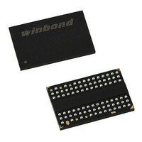
W9751G6IB-25 Winbond Electronics, W9751G6IB-25 Datasheet - Page 29

W9751G6IB-25
Manufacturer Part Number
W9751G6IB-25
Description
IC DDR2-800 SDRAM 512MB 84-WBGA
Manufacturer
Winbond Electronics
Datasheet
1.W9751G6IB-25.pdf
(86 pages)
Specifications of W9751G6IB-25
Format - Memory
RAM
Memory Type
DDR2 SDRAM
Memory Size
512M (32Mx16)
Speed
2.5ns
Interface
Parallel
Voltage - Supply
1.7 V ~ 1.9 V
Operating Temperature
0°C ~ 85°C
Package / Case
84-WBGA
Lead Free Status / RoHS Status
Lead free / RoHS Compliant
Available stocks
Company
Part Number
Manufacturer
Quantity
Price
Company:
Part Number:
W9751G6IB-25
Manufacturer:
WINBOND
Quantity:
15
Company:
Part Number:
W9751G6IB-25
Manufacturer:
WINBOND
Quantity:
1 248
Company:
Part Number:
W9751G6IB-25
Manufacturer:
Winbond Electronics
Quantity:
10 000
Part Number:
W9751G6IB-25
Manufacturer:
WINBOND/华邦
Quantity:
20 000
Notes:
1. RTP[cycles] = RU{ tRTP[nS] / tCK(avg)[nS] }, where RU stands for round up.
2. For a given bank, the precharge period should be counted from the latest precharge command, either one bank precharge or
7.8
Two types of Refresh operation can be performed on the device: Auto Refresh and Self Refresh. By
repeating the Auto Refresh cycle, each bank in turn refreshed automatically. The Refresh operation
must be performed 8192 times (rows) within 64mS. The period between the Auto Refresh command
and the next command is specified by t
Self Refresh mode enters issuing the Self Refresh command (CKE asserted "LOW") while all banks
are in the idle state. The device is in Self Refresh mode for as long as CKE held "LOW". In the case
of 8192 burst Auto Refresh commands, 8192 burst Auto Refresh commands must be performed within
7.8 µS before entering and after exiting the Self Refresh mode. In the case of distributed Auto Refresh
commands, distributed auto refresh commands must be issued every 7.8 µS and the last distributed
Auto Refresh commands must be performed within 7.8 µS before entering the self refresh mode. After
exiting from the Self Refresh mode, the refresh operation must be performed within 7.8 µS. In Self
Refresh mode, all input/output buffers are disable, resulting in lower power dissipation (except CKE
buffer). (Example timing waveform refer to 10.29 Self Refresh diagram in Chapter 10)
7.9
Power-down is synchronously entered when CKE is registered LOW, along with NOP or Deselect
command. CKE is not allowed to go LOW while mode register or extended mode register command
time, or read or write operation is in progress. CKE is allowed to go LOW while any other operation
such as row activation, Precharge or Auto-precharge or Auto Refresh is in progress, but power down
I
The DLL should be in a locked state when power-down is entered. Otherwise DLL should be reset
after exiting power-down mode for proper read operation.
Command
Read w/AP
Write w/AP
DD
Precharge
Precharge
precharge all, issued to that bank. The precharge period is satisfied after t
issued to that bank.
From
Read
Write
specification will not be applied until finishing those operations.
All
Refresh Operation
Power Down Mode
Precharge (to same Bank as Read w/AP)
Precharge (to same Bank as Write w/AP)
Precharge (to same Bank as Precharge)
Precharge (to same Bank as Read)
Precharge (to same Bank as Write)
Table 5—Precharge & Auto-precharge clarifications
To Command
Precharge All
Precharge All
Precharge All
Precharge All
Precharge All
Precharge All
Precharge
RFC
.
- 29 -
Minimum Delay between “From
Command” to “To Command”
AL + BL/2 + max(RTP, 2) - 2
AL + BL/2 + max(RTP, 2) - 2
AL + BL/2 + max(RTP, 2) - 2
AL + BL/2 + max(RTP, 2) - 2
RP
WL + BL/2 + t
WL + BL/2 + t
WL + BL/2 + WR
WL + BL/2 + WR
depending on the latest precharge command
Publication Release Date: Oct. 23, 2009
1
1
1
1
WR
WR
W9751G6IB
Unit
clks
clks
clks
clks
clks
clks
clks
clks
clks
clks
clks
clks
Revision A06
Notes
1, 2
1, 2
1, 2
1, 2
2
2
2
2
2
2
2
2


