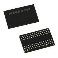
W9751G6IB-25 Winbond Electronics, W9751G6IB-25 Datasheet - Page 49

W9751G6IB-25
Manufacturer Part Number
W9751G6IB-25
Description
IC DDR2-800 SDRAM 512MB 84-WBGA
Manufacturer
Winbond Electronics
Datasheet
1.W9751G6IB-25.pdf
(86 pages)
Specifications of W9751G6IB-25
Format - Memory
RAM
Memory Type
DDR2 SDRAM
Memory Size
512M (32Mx16)
Speed
2.5ns
Interface
Parallel
Voltage - Supply
1.7 V ~ 1.9 V
Operating Temperature
0°C ~ 85°C
Package / Case
84-WBGA
Lead Free Status / RoHS Status
Lead free / RoHS Compliant
Available stocks
Company
Part Number
Manufacturer
Quantity
Price
Company:
Part Number:
W9751G6IB-25
Manufacturer:
WINBOND
Quantity:
15
Company:
Part Number:
W9751G6IB-25
Manufacturer:
WINBOND
Quantity:
1 248
Company:
Part Number:
W9751G6IB-25
Manufacturer:
Winbond Electronics
Quantity:
10 000
Part Number:
W9751G6IB-25
Manufacturer:
WINBOND/华邦
Quantity:
20 000
18. User can choose which active power down exit timing to use via MRS (bit 12). tXARD is expected to be used for fast active
19. AL = Additive Latency.
20. ODT turn on time min is when the device leaves high impedance and ODT resistance begins to turn on. ODT turn on time
21. ODT turn off time min is when the device starts to turn off ODT resistance. ODT turn off time max is when the bus is in high
22. The clock frequency is allowed to change during Self Refresh mode or precharge power-down mode. In case of clock
23. For these parameters, the DDR2 SDRAM device is characterized and verified to support tnPARAM = RU{tPARAM /
24. tDAL [nCK] = WR [nCK] + tnRP [nCK] = WR + RU {tRP [pS] / tCK(avg) [pS] }, where WR is the value programmed in the
25. New units, ‘tCK(avg)’ and ‘nCK’, are introduced in DDR2-667 and DDR2-800.
26. These parameters are measured from a command/address signal (CKE, CS , RAS , CAS , WE , ODT, BA0, A0, A1, etc.)
Logic levels
V
REF
power down exit timing. tXARDS is expected to be used for slow active power down exit timing.
max is when the ODT resistance is fully on. Both are measure from tAOND, which is interpreted differently per speed bin.
For DDR2-667/800, tAOND is 2 clock cycles after the clock edge that registered a first ODT HIGH counting the actual input
clock edges.
impedance. Both are measured from tAOFD.
frequency change during precharge power-down, a specific procedure is required as described in section 7.10.
tCK(avg)}, which is in clock cycles, assuming all input clock jitter specifications are satisfied.
mode register set and RU stands for round up.
transition edge to its respective clock signal (CLK/ CLK ) crossing. The spec values are not affected by the amount of clock
jitter applied (i.e. tJIT(per), tJIT(cc), etc.), as the setup and hold are relative to the clock signal crossing that latches the
command/address. That is, these parameters should be met whether clock jitter is present or not.
DQS
DQS
levels
Figure 19 — Differential input waveform timing – tDS and tDH
For DDR2-667/800: This is interpreted differently per speed bin. If tCK(avg) = 3 nS is assumed, tAOFD is 1.5 nS (=
0.5 x 3 nS) after the second trailing clock edge counting from the clock edge that registered a first ODT LOW and by
counting the actual input clock edges.
Example:
The device will support tnRP = RU{tRP / tCK(avg)}, which is in clock cycles, if all input clock jitter specifications are
met. This means: For DDR2-667 5-5-5, of which tRP = 15nS, the device will support tnRP = RU{tRP / tCK(avg)} = 5,
i.e. as long as the input clock jitter specifications are met, Precharge command at Tm and Active command at Tm+5
is valid even if (Tm+5 - Tm) is less than 15nS due to input clock jitter.
Unit ‘tCK(avg)’ represents the actual tCK(avg) of the input clock under operation.
Unit ‘nCK’ represents one clock cycle of the input clock, counting the actual clock edges.
Example:
For DDR2-667/800: tXP = 2 [nCK] means; if Power Down exit is registered at Tm, an Active command may be
registered at Tm+2, even if (Tm+2 - Tm) is 2 x tCK(avg) + tERR(2per),min.
t
t
DS(ref)
DS(base)
t
DH(base)
t
DH(ref)
t
t
DS(ref)
DS(base)
- 49 -
t
DH(base)
t
DH(ref)
Publication Release Date: Oct. 23, 2009
V
V
V
V
V
V
V
DDQ
IH(ac)
IH(dc)
REF(dc)
IL(dc)
IL(ac)
SS
W9751G6IB
max
max
min
min
Revision A06


