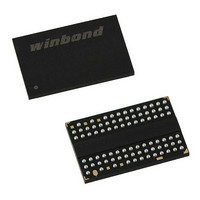
W9751G6IB-25 Winbond Electronics, W9751G6IB-25 Datasheet - Page 11

W9751G6IB-25
Manufacturer Part Number
W9751G6IB-25
Description
IC DDR2-800 SDRAM 512MB 84-WBGA
Manufacturer
Winbond Electronics
Datasheet
1.W9751G6IB-25.pdf
(86 pages)
Specifications of W9751G6IB-25
Format - Memory
RAM
Memory Type
DDR2 SDRAM
Memory Size
512M (32Mx16)
Speed
2.5ns
Interface
Parallel
Voltage - Supply
1.7 V ~ 1.9 V
Operating Temperature
0°C ~ 85°C
Package / Case
84-WBGA
Lead Free Status / RoHS Status
Lead free / RoHS Compliant
Available stocks
Company
Part Number
Manufacturer
Quantity
Price
Company:
Part Number:
W9751G6IB-25
Manufacturer:
WINBOND
Quantity:
15
Company:
Part Number:
W9751G6IB-25
Manufacturer:
WINBOND
Quantity:
1 248
Company:
Part Number:
W9751G6IB-25
Manufacturer:
Winbond Electronics
Quantity:
10 000
Part Number:
W9751G6IB-25
Manufacturer:
WINBOND/华邦
Quantity:
20 000
SDRAM. Burst address sequence type is defined by A3, CAS Latency is defined by A[6:4]. The DDR2
does not support half clock latency mode. A7 is used for test mode. A8 is used for DLL reset. A7 must
be set to LOW for normal MRS operation. Write recovery time WR is defined by A[11:9]. Refer to the
table for specific codes.
Note:
1. WR min is determined by tCK(avg) max and WR max is determined by tCK(avg) min. WR[cycles] = RU{ tWR[nS] /
7.2.2
7.2.2.1
( CS = "L", RAS = "L", CAS = "L", WE = "L", BA0 = "H", BA1 = "L", A0 to A12 = Register data)
The extended mode register (1) stores the data for enabling or disabling the DLL, output driver
strength, additive latency, ODT, DQS disable, OCD program. The default value of the extended
mode register (1) is not defined, therefore the extended mode register (1) must be programmed during
initialization for proper operation. The DDR2 SDRAM should be in all bank precharge with CKE
already high prior to writing into the extended mode register (1). The mode register set command
cycle time (t
Extended mode register (1) contents can be changed using the same command and clock cycle
requirements during normal operation as long as all banks are in the precharge state. A0 is used for
DLL enable or disable. A1 is used for enabling a reduced strength output driver. A[5:3] determines the
additive latency, A[9:7] are used for OCD control, A10 is used for DQS disable. A2 and A6 are used
for ODT setting.
tCK(avg)[nS] }, where RU stands for round up. The mode register must be programmed to this value. This is also used with
tRP to determine tDAL.
BA1
0
0
1
1
BA0
0
1
0
1
Extend Mode Register Set Commands (EMRS)
A12
Extend Mode Register Set Command (1), EMR (1)
0
1
MRD
A8
0
1
MRS mode
Active power down exit time
EMR (1)
EMR (2)
EMR (3)
BA1
Slow exit (use t
) must be satisfied to complete the write operation to the extended mode register (1).
MR
0
Fast exit (use t
DLL Reset
Yes
No
BA0
0
A12
PD
XARDS
XARD
A11
)
)
Figure 2—Mode Register Set (MRS)
A10
WR
Write recovery for Auto-precharge
A11
0
0
0
0
1
1
1
1
A9
A10
0
0
1
1
0
0
1
1
DLL
A8
A7
0
1
A9
0
1
0
1
0
1
0
1
TM
A7
Normal
Mode
Test
Reserved
Reserved
Reserved
- 11 -
WR *
A6
CAS Latency
2
3
4
5
6
A5
A4
A3
BT
A3
0
1
Publication Release Date: Oct. 23, 2009
A2
Burst Length
Burst Type
Sequential
Interleave
A6
0
0
0
0
1
1
1
1
A1
CAS Latency
A5
0
0
1
1
0
0
1
1
A0
A4
0
1
0
1
0
1
0
1
W9751G6IB
A2
0
0
Burst Length
Address Field
Mode Register
Reserved
Reserved
Reserved
Reserved
Latency
A1
1
1
3
4
5
6
Revision A06
A0
0
1
BL
4
8


