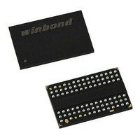
W9751G6IB-25 Winbond Electronics, W9751G6IB-25 Datasheet - Page 26

W9751G6IB-25
Manufacturer Part Number
W9751G6IB-25
Description
IC DDR2-800 SDRAM 512MB 84-WBGA
Manufacturer
Winbond Electronics
Datasheet
1.W9751G6IB-25.pdf
(86 pages)
Specifications of W9751G6IB-25
Format - Memory
RAM
Memory Type
DDR2 SDRAM
Memory Size
512M (32Mx16)
Speed
2.5ns
Interface
Parallel
Voltage - Supply
1.7 V ~ 1.9 V
Operating Temperature
0°C ~ 85°C
Package / Case
84-WBGA
Lead Free Status / RoHS Status
Lead free / RoHS Compliant
Available stocks
Company
Part Number
Manufacturer
Quantity
Price
Company:
Part Number:
W9751G6IB-25
Manufacturer:
WINBOND
Quantity:
15
Company:
Part Number:
W9751G6IB-25
Manufacturer:
WINBOND
Quantity:
1 248
Company:
Part Number:
W9751G6IB-25
Manufacturer:
Winbond Electronics
Quantity:
10 000
Part Number:
W9751G6IB-25
Manufacturer:
WINBOND/华邦
Quantity:
20 000
7.4.5
One write data mask (DM) pin for each 8 data bits (DQ) will be supported on DDR2 SDRAM,
consistent with the implementation on DDR1 SDRAM. It has identical timings on write operations as
the data bits, and though used in a unidirectional manner, is internally loaded identically to data bits to
insure matched system timing. DM is not used during read cycles. (Example timing waveform refer to
10.15 Write operation with Data Mask diagram in Chapter 10)
7.5
Read or Write burst interruption is prohibited for burst length of 4 and only allowed for burst length of 8
under the following conditions:
(Example timing waveforms refer to 10.13 and 10.14 Burst read and write interrupt timing diagram in
Chapter 10)
1. Read burst of 8 can only be interrupted by another Read command. Read burst interruption by
2. Write burst of 8 can only be interrupted by another Write command. Write burst interruption by
3. Read burst interrupt must occur exactly two clocks after the previous Read command. Any other
4. Write burst interrupt must occur exactly two clocks after the previous Write command. Any other
5. Read or Write burst interruption is allowed to any bank inside the DDR2 SDRAM.
6. Read or Write burst with Auto-precharge enabled is not allowed to interrupt.
7. Read burst interruption is allowed by a Read with Auto-precharge command.
8. Write burst interruption is allowed by a Write with Auto-precharge command.
9. All command timings are referenced to burst length set in the mode register. They are not
Burst Interrupt
Write or Precharge Command is prohibited.
Read or Precharge Command is prohibited.
Read burst interrupt timings are prohibited.
Write burst interrupt timings are prohibited.
referenced to the actual burst. For example below:
Write data mask
Minimum Read to Precharge timing is AL + BL/2 where BL is the burst length set in the
mode register and not the actual burst (which is shorter because of interrupt).
Minimum Write to Precharge timing is WL + BL/ 2 + t
clock after the un-interrupted burst end and not from the end of the actual burst end.
- 26 -
WR
Publication Release Date: Oct. 23, 2009
, where t
WR
W9751G6IB
starts with the rising
Revision A06


