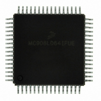
MC908LD64IFUE Freescale Semiconductor, MC908LD64IFUE Datasheet - Page 167

MC908LD64IFUE
Manufacturer Part Number
MC908LD64IFUE
Description
IC MCU 8BIT FOR LCD 64-QFP
Manufacturer
Freescale Semiconductor
Series
HC08r
Datasheet
1.MC908LD64IFUE.pdf
(362 pages)
Specifications of MC908LD64IFUE
Core Processor
HC08
Core Size
8-Bit
Speed
6MHz
Connectivity
I²C, USB
Peripherals
OSD, POR, PWM
Number Of I /o
39
Program Memory Size
60KB (60K x 8)
Program Memory Type
FLASH
Ram Size
2K x 8
Voltage - Supply (vcc/vdd)
3 V ~ 3.6 V
Data Converters
A/D 6x8b
Oscillator Type
Internal
Operating Temperature
0°C ~ 85°C
Package / Case
64-QFP
Processor Series
HC08LD
Core
HC08
Data Bus Width
8 bit
Data Ram Size
2 KB
Interface Type
I2C, USB
Maximum Clock Frequency
6 MHz
Number Of Programmable I/os
39
Number Of Timers
2
Maximum Operating Temperature
+ 85 C
Mounting Style
SMD/SMT
Development Tools By Supplier
FSICEBASE, M68CBL05CE
Minimum Operating Temperature
0 C
On-chip Adc
8 bit, 6 Channel
Lead Free Status / RoHS Status
Lead free / RoHS Compliant
Eeprom Size
-
Lead Free Status / Rohs Status
Details
Available stocks
Company
Part Number
Manufacturer
Quantity
Price
Company:
Part Number:
MC908LD64IFUE
Manufacturer:
Freescale Semiconductor
Quantity:
10 000
Part Number:
MC908LD64IFUE
Manufacturer:
FREESCALE
Quantity:
20 000
- Current page: 167 of 362
- Download datasheet (2Mb)
MC68HC908LD64
Freescale Semiconductor
NOTE:
NOTE:
—
Rev. 3.0
Before changing a channel function by writing to the MSxB or MSxA bit,
set the TSTOP and TRST bits in the TIM status and control register
(TSC).
ELSxB and ELSxA — Edge/Level Select Bits
Before enabling a TIM channel register for input capture operation, make
sure that the TCHx pin is stable for at least two bus clocks.
Notes:
MSxB
1. For CLAMP/TCH0 pin only.
When channel x is an input capture channel, these read/write bits
control the active edge-sensing logic on channel x.
When channel x is an output compare channel, ELSxB and ELSxA
control the channel x output behavior when an output compare
occurs.
When ELS0B and ELS0A are both clear, channel 0 is not connected
to the CLAMP/TCH0 pin. The pin is available as the CLAMP output of
the sync processor.
Table 11-3
ELSxB and ELSxA bits.
X
X
0
0
0
0
0
0
1
1
1
MSxA
0
1
0
0
0
1
1
1
X
X
X
Timer Interface Module (TIM)
Table 11-3. Mode, Edge, and Level Selection
shows how ELSxB and ELSxA work. Reset clears the
ELSxB
0
0
0
1
1
0
1
1
0
1
1
ELSxA
0
0
1
0
1
1
0
1
1
0
1
Compare or
Compare
Capture
or PWM
Buffered
Buffered
Output
Output
Mode
Preset
Output
Input
PWM
Pin is CLAMP of sync processor
Initial Output Level High
Pin is CLAMP of sync processor
Initial Output Level Low
Capture on Rising Edge Only
Capture on Falling Edge Only
Capture on Rising or Falling Edge
Toggle Output on Compare
Clear Output on Compare
Set Output on Compare
Toggle Output on Compare
Clear Output on Compare
Set Output on Compare
Timer Interface Module (TIM)
Configuration
I/O Registers
Data Sheet
(1)
(1)
167
;
;
Related parts for MC908LD64IFUE
Image
Part Number
Description
Manufacturer
Datasheet
Request
R
Part Number:
Description:
Manufacturer:
Freescale Semiconductor, Inc
Datasheet:
Part Number:
Description:
Manufacturer:
Freescale Semiconductor, Inc
Datasheet:
Part Number:
Description:
Manufacturer:
Freescale Semiconductor, Inc
Datasheet:
Part Number:
Description:
Manufacturer:
Freescale Semiconductor, Inc
Datasheet:
Part Number:
Description:
Manufacturer:
Freescale Semiconductor, Inc
Datasheet:
Part Number:
Description:
Manufacturer:
Freescale Semiconductor, Inc
Datasheet:
Part Number:
Description:
Manufacturer:
Freescale Semiconductor, Inc
Datasheet:
Part Number:
Description:
Manufacturer:
Freescale Semiconductor, Inc
Datasheet:
Part Number:
Description:
Manufacturer:
Freescale Semiconductor, Inc
Datasheet:
Part Number:
Description:
Manufacturer:
Freescale Semiconductor, Inc
Datasheet:
Part Number:
Description:
Manufacturer:
Freescale Semiconductor, Inc
Datasheet:
Part Number:
Description:
Manufacturer:
Freescale Semiconductor, Inc
Datasheet:
Part Number:
Description:
Manufacturer:
Freescale Semiconductor, Inc
Datasheet:
Part Number:
Description:
Manufacturer:
Freescale Semiconductor, Inc
Datasheet:
Part Number:
Description:
Manufacturer:
Freescale Semiconductor, Inc
Datasheet:


