MC908LD64IFUE Freescale Semiconductor, MC908LD64IFUE Datasheet - Page 72
MC908LD64IFUE
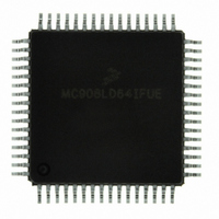
Manufacturer Part Number
MC908LD64IFUE
Description
IC MCU 8BIT FOR LCD 64-QFP
Manufacturer
Freescale Semiconductor
Series
HC08r
Datasheet
1.MC908LD64IFUE.pdf
(362 pages)
Specifications of MC908LD64IFUE
Core Processor
HC08
Core Size
8-Bit
Speed
6MHz
Connectivity
I²C, USB
Peripherals
OSD, POR, PWM
Number Of I /o
39
Program Memory Size
60KB (60K x 8)
Program Memory Type
FLASH
Ram Size
2K x 8
Voltage - Supply (vcc/vdd)
3 V ~ 3.6 V
Data Converters
A/D 6x8b
Oscillator Type
Internal
Operating Temperature
0°C ~ 85°C
Package / Case
64-QFP
Processor Series
HC08LD
Core
HC08
Data Bus Width
8 bit
Data Ram Size
2 KB
Interface Type
I2C, USB
Maximum Clock Frequency
6 MHz
Number Of Programmable I/os
39
Number Of Timers
2
Maximum Operating Temperature
+ 85 C
Mounting Style
SMD/SMT
Development Tools By Supplier
FSICEBASE, M68CBL05CE
Minimum Operating Temperature
0 C
On-chip Adc
8 bit, 6 Channel
Lead Free Status / RoHS Status
Lead free / RoHS Compliant
Eeprom Size
-
Lead Free Status / Rohs Status
Details
Available stocks
Company
Part Number
Manufacturer
Quantity
Price
Company:

Part Number:
MC908LD64IFUE
Manufacturer:
Freescale Semiconductor
Quantity:
10 000
Part Number:
MC908LD64IFUE
Manufacturer:
FREESCALE
Quantity:
20 000


FLASH Memory
4.8 FLASH Block Protection
4.8.1 FLASH Block Protect Registers
Data Sheet
72
Address:
Address:
Due to the ability of the on-board charge pump to erase and program the
FLASH memory in the target application, provision is made for protecting
blocks of memory from unintentional erase or program operations due to
system malfunction. This protection is done by use of a FLASH Block
Protect Register for each array (FLBPR and FLBPR1). The block protect
register determines the range of the FLASH memory which is to be
protected. The range of the protected area starts from a location defined
by block protect register and ends at the bottom of the FLASH memory
array ($FFFF and $3FFF). When the memory is protected, the HVEN bit
cannot be set in either ERASE or PROGRAM operations.
Each FLASH block protect register is implemented as an 7-bit I/O
register. The BPR bit content of the register determines the starting
location of the protected range within the FLASH memory.
This register controls the 47,616-byte array:
This register controls the 13K-byte array:
Figure 4-7. 13K-byte FLASH Block Protect Register 1 (FLBPR1)
Reset:
Figure 4-6. 47,616-byte FLASH Block Protect Register (FLBPR)
Reset:
Read:
Write:
Read:
Write:
$FE0B
BPR17
$FE08
BPR7
Bit 7
Bit 7
0
0
BPR16
BPR6
FLASH Memory
6
0
6
0
BPR15
BPR5
5
0
5
0
BPR14
BPR4
4
0
4
0
BPR13
BPR3
3
0
3
0
MC68HC908LD64
BPR12
BPR2
Freescale Semiconductor
2
0
2
0
BPR11
BPR1
1
0
1
0
—
Rev. 3.0
Bit 0
Bit 0
0
0
0
0
Related parts for MC908LD64IFUE
Image
Part Number
Description
Manufacturer
Datasheet
Request
R

Part Number:
Description:
Manufacturer:
Freescale Semiconductor, Inc
Datasheet:
Part Number:
Description:
Manufacturer:
Freescale Semiconductor, Inc
Datasheet:
Part Number:
Description:
Manufacturer:
Freescale Semiconductor, Inc
Datasheet:
Part Number:
Description:
Manufacturer:
Freescale Semiconductor, Inc
Datasheet:
Part Number:
Description:
Manufacturer:
Freescale Semiconductor, Inc
Datasheet:
Part Number:
Description:
Manufacturer:
Freescale Semiconductor, Inc
Datasheet:
Part Number:
Description:
Manufacturer:
Freescale Semiconductor, Inc
Datasheet:
Part Number:
Description:
Manufacturer:
Freescale Semiconductor, Inc
Datasheet:
Part Number:
Description:
Manufacturer:
Freescale Semiconductor, Inc
Datasheet:
Part Number:
Description:
Manufacturer:
Freescale Semiconductor, Inc
Datasheet:
Part Number:
Description:
Manufacturer:
Freescale Semiconductor, Inc
Datasheet:
Part Number:
Description:
Manufacturer:
Freescale Semiconductor, Inc
Datasheet:
Part Number:
Description:
Manufacturer:
Freescale Semiconductor, Inc
Datasheet:
Part Number:
Description:
Manufacturer:
Freescale Semiconductor, Inc
Datasheet:
Part Number:
Description:
Manufacturer:
Freescale Semiconductor, Inc
Datasheet: