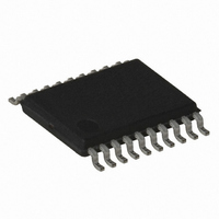
ATTINY167-15XD Atmel, ATTINY167-15XD Datasheet - Page 100

ATTINY167-15XD
Manufacturer Part Number
ATTINY167-15XD
Description
MCU AVR 16K FLASH 15MHZ 20-TSSOP
Manufacturer
Atmel
Series
AVR® ATtinyr
Datasheet
1.ATTINY167-15MD.pdf
(283 pages)
Specifications of ATTINY167-15XD
Core Processor
AVR
Core Size
8-Bit
Speed
16MHz
Connectivity
I²C, LIN, SPI, UART/USART, USI
Peripherals
Brown-out Detect/Reset, POR, PWM, Temp Sensor, WDT
Number Of I /o
16
Program Memory Size
16KB (8K x 16)
Program Memory Type
FLASH
Eeprom Size
512 x 8
Ram Size
512 x 8
Voltage - Supply (vcc/vdd)
2.7 V ~ 5.5 V
Data Converters
A/D 11x10b
Oscillator Type
Internal
Operating Temperature
-40°C ~ 150°C
Package / Case
20-TSSOP
Processor Series
ATTINY1x
Core
AVR8
Data Bus Width
8 bit
Data Ram Size
512 B
Maximum Clock Frequency
16 MHz
Maximum Operating Temperature
+ 85 C
Mounting Style
SMD/SMT
3rd Party Development Tools
EWAVR, EWAVR-BL
Development Tools By Supplier
ATAVRDRAGON, ATSTK500, ATSTK600, ATAVRISP2, ATAVRONEKIT
Minimum Operating Temperature
- 40 C
For Use With
ATSTK600-SOIC - STK600 SOCKET/ADAPTER FOR SOIC
Lead Free Status / RoHS Status
Lead free / RoHS Compliant
- Current page: 100 of 283
- Download datasheet (5Mb)
10.10 Timer/Counter0 Prescaler
10.11 8-bit Timer/Counter Register Description
100
ATtiny87/ATtiny167
Figure 10-12. Prescaler for Timer/Counter0
The clock source for Timer/Counter0 is named clk
main system I/O clock clk
nously clocked from the XTAL oscillator or XTAL1 pin. This enables use of Timer/Counter0 as
a Real Time Counter (RTC).
A crystal can then be connected between the XTAL1 and XTAL2 pins to serve as an indepen-
dent clock source for Timer/Counter0.
A external clock can also be used using XTAL1 as input. Setting AS0 and EXCLK enables this
configuration.
For Timer/Counter0, the possible prescaled selections are: clk
clk
selected. Setting the PSR0 bit in GTCCR resets the prescaler. This allows the user to operate
with a predictable prescaler.
• Timer/Counter0 Control Register A – TCCR0A
• Bit 7:6 – COM0A1:0: Compare Match Output Mode A
These bits control the Output Compare pin (OC0A) behavior. If one or both of the COM0A1:0
bits are set, the OC0A output overrides the normal port functionality of the I/O pin it is con-
nected to. However, note that the Data Direction Register (DDR) bit corresponding to OC0A
pin must be set in order to enable the output driver.
Bit
Read/Write
Initial Value
T
0
XTAL2
XTAL1
S
/128, clk
COM0A1
T
R/W
Oscillator
0
7
0
S
/256, and clk
EXCLK
PSRn
CSn0
CSn1
CSn2
COM0A0
R/W
6
0
clk
IO
0
1
I/O
. By setting the AS0 bit in ASSR, Timer/Counter0 is asynchro-
ASn
T
0
R
5
–
0
S
0
1
/1024. Additionally, clk
clk
TnS
4
–
R
0
Clear
T
0
TIMER/COUNTERn CLOCK SOURCE
3
–
R
0
S
. clk
0
T
0
T
10-BIT T/C PRESCALER
S
0
R
2
–
0
S
is by default connected to the
clk
as well as 0 (stop) may be
T
Tn
0
S
WGM01
/8, clk
R/W
1
0
T
0
S
WGM00
/32, clk
R/W
7728G–AVR–06/10
0
0
T
TCCR0A
0
S
/64,
Related parts for ATTINY167-15XD
Image
Part Number
Description
Manufacturer
Datasheet
Request
R

Part Number:
Description:
Manufacturer:
Atmel Corporation
Datasheet:

Part Number:
Description:
Manufacturer:
Atmel Corporation
Datasheet:

Part Number:
Description:
MCU AVR 16K FLASH 15MHZ 32-QFN
Manufacturer:
Atmel
Datasheet:

Part Number:
Description:
IC MCU AVR 16K FLASH 20TSSOP
Manufacturer:
Atmel
Datasheet:

Part Number:
Description:
MCU AVR 16K FLASH 15MHZ 32-QFN
Manufacturer:
Atmel
Datasheet:

Part Number:
Description:
MCU AVR 16K FLASH 15MHZ 20-SOIC
Manufacturer:
Atmel
Datasheet:

Part Number:
Description:
MCU AVR 16K FLASH 15MHZ 20-TSSOP
Manufacturer:
Atmel
Datasheet:

Part Number:
Description:
IC MCU AVR 16K FLASH 20SOIC
Manufacturer:
Atmel
Datasheet:


