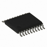
ATTINY167-15XD Atmel, ATTINY167-15XD Datasheet - Page 210

ATTINY167-15XD
Manufacturer Part Number
ATTINY167-15XD
Description
MCU AVR 16K FLASH 15MHZ 20-TSSOP
Manufacturer
Atmel
Series
AVR® ATtinyr
Datasheet
1.ATTINY167-15MD.pdf
(283 pages)
Specifications of ATTINY167-15XD
Core Processor
AVR
Core Size
8-Bit
Speed
16MHz
Connectivity
I²C, LIN, SPI, UART/USART, USI
Peripherals
Brown-out Detect/Reset, POR, PWM, Temp Sensor, WDT
Number Of I /o
16
Program Memory Size
16KB (8K x 16)
Program Memory Type
FLASH
Eeprom Size
512 x 8
Ram Size
512 x 8
Voltage - Supply (vcc/vdd)
2.7 V ~ 5.5 V
Data Converters
A/D 11x10b
Oscillator Type
Internal
Operating Temperature
-40°C ~ 150°C
Package / Case
20-TSSOP
Processor Series
ATTINY1x
Core
AVR8
Data Bus Width
8 bit
Data Ram Size
512 B
Maximum Clock Frequency
16 MHz
Maximum Operating Temperature
+ 85 C
Mounting Style
SMD/SMT
3rd Party Development Tools
EWAVR, EWAVR-BL
Development Tools By Supplier
ATAVRDRAGON, ATSTK500, ATSTK600, ATAVRISP2, ATAVRONEKIT
Minimum Operating Temperature
- 40 C
For Use With
ATSTK600-SOIC - STK600 SOCKET/ADAPTER FOR SOIC
Lead Free Status / RoHS Status
Lead free / RoHS Compliant
- Current page: 210 of 283
- Download datasheet (5Mb)
17.11.6
17.11.7
210
ATtiny87/ATtiny167
DIDR1 – Digital Input Disable Register 1
AMISCR – Analog Miscellaneous Control Register
• Bits 7:0 – ADC7D:ADC0D: ADC7:0 Digital Input Disable
When this bit is written logic one, the digital input buffer on the corresponding ADC pin is dis-
abled. The corresponding PIN register bit will always read as zero when this bit is set. When
an analog signal is applied to the ADC7:0 pin and the digital input from this pin is not needed,
this bit should be written logic one to reduce power consumption in the digital input buffer.
• Bit 7 – Res: Reserved Bit
This bit is reserved for future use. For compatibility with future devices it must be written to
zero when DIDR1 register is written.
• Bits 6..4 – ADC10D..ADC8D: ADC10..8 Digital Input Disable
When this bit is written logic one, the digital input buffer on the corresponding ADC pin is dis-
abled. The corresponding PIN register bit will always read as zero when this bit is set. When
an analog signal is applied to the ADC10:8 pin and the digital input from this pin is not needed,
this bit should be written logic one to reduce power consumption in the digital input buffer.
• Bits 3:0 - Reserved Bits
These bits are reserved for future use. For compatibility with future devices, they must be writ-
ten to zero when DIDR1 is written.
• Bits 7:3 – Reserved Bits
These bits are reserved for future use. For compatibility with future devices, they must be writ-
ten to zero when AMISCR is written.
• Bit 2 – AREFEN: External Voltage Reference Input Enable
When this bit is written logic one, the voltage reference for the ADC is input from AREF pin as
described in
AREF higher than (AVcc - 1V) is not recommended, as this will affect ADC accuracy. The
internal voltage reference options may not be used if an external voltage is being applied to
the AREF pin. It is recommended to use DIDR register bit function (digital input disable) when
AREFEN is set.
• Bit 1 – XREFEN: Internal Voltage Reference Output Enable
When this bit is written logic one, the internal voltage reference 1.1V or 2.56V is output on
XREF pin as described in
bit function (digital input disable) when XREFEN is set.
Bit
Read/Write
Initial Value
Bit
Read/Write
Initial Value
Table 17.10 on page
R
R
7
0
7
0
-
-
ADC10D
R/W
R
6
0
6
0
-
Table 17.10 on page
ADC9D
R/W
204. If active channels are used, using AVcc or an external
R
5
0
5
0
-
ADC8D
R/W
R
4
0
4
0
-
204. It is recommended to use DIDR register
R
R
3
0
3
0
-
-
AREFEN
R/W
R
2
0
-
2
0
XREFEN
R/W
R
1
0
-
1
0
ISRCEN
R/W
R
0
0
-
0
0
7728G–AVR–06/10
AMISCR
DIDR1
Related parts for ATTINY167-15XD
Image
Part Number
Description
Manufacturer
Datasheet
Request
R

Part Number:
Description:
Manufacturer:
Atmel Corporation
Datasheet:

Part Number:
Description:
Manufacturer:
Atmel Corporation
Datasheet:

Part Number:
Description:
MCU AVR 16K FLASH 15MHZ 32-QFN
Manufacturer:
Atmel
Datasheet:

Part Number:
Description:
IC MCU AVR 16K FLASH 20TSSOP
Manufacturer:
Atmel
Datasheet:

Part Number:
Description:
MCU AVR 16K FLASH 15MHZ 32-QFN
Manufacturer:
Atmel
Datasheet:

Part Number:
Description:
MCU AVR 16K FLASH 15MHZ 20-SOIC
Manufacturer:
Atmel
Datasheet:

Part Number:
Description:
MCU AVR 16K FLASH 15MHZ 20-TSSOP
Manufacturer:
Atmel
Datasheet:

Part Number:
Description:
IC MCU AVR 16K FLASH 20SOIC
Manufacturer:
Atmel
Datasheet:


