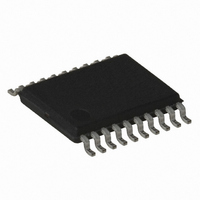
ATTINY167-15XD Atmel, ATTINY167-15XD Datasheet - Page 125

ATTINY167-15XD
Manufacturer Part Number
ATTINY167-15XD
Description
MCU AVR 16K FLASH 15MHZ 20-TSSOP
Manufacturer
Atmel
Series
AVR® ATtinyr
Datasheet
1.ATTINY167-15MD.pdf
(283 pages)
Specifications of ATTINY167-15XD
Core Processor
AVR
Core Size
8-Bit
Speed
16MHz
Connectivity
I²C, LIN, SPI, UART/USART, USI
Peripherals
Brown-out Detect/Reset, POR, PWM, Temp Sensor, WDT
Number Of I /o
16
Program Memory Size
16KB (8K x 16)
Program Memory Type
FLASH
Eeprom Size
512 x 8
Ram Size
512 x 8
Voltage - Supply (vcc/vdd)
2.7 V ~ 5.5 V
Data Converters
A/D 11x10b
Oscillator Type
Internal
Operating Temperature
-40°C ~ 150°C
Package / Case
20-TSSOP
Processor Series
ATTINY1x
Core
AVR8
Data Bus Width
8 bit
Data Ram Size
512 B
Maximum Clock Frequency
16 MHz
Maximum Operating Temperature
+ 85 C
Mounting Style
SMD/SMT
3rd Party Development Tools
EWAVR, EWAVR-BL
Development Tools By Supplier
ATAVRDRAGON, ATSTK500, ATSTK600, ATAVRISP2, ATAVRONEKIT
Minimum Operating Temperature
- 40 C
For Use With
ATSTK600-SOIC - STK600 SOCKET/ADAPTER FOR SOIC
Lead Free Status / RoHS Status
Lead free / RoHS Compliant
- Current page: 125 of 283
- Download datasheet (5Mb)
7728G–AVR–06/10
In fast PWM mode the counter is incremented until the counter value matches either one of
the fixed values 0x00FF, 0x01FF, or 0x03FF (WGM13:0 = 5, 6, or 7), the value in ICR1
(WGM13:0 = 14), or the value in OCR1A (WGM13:0 = 15). The counter is then cleared at the
following timer clock cycle. The timing diagram for the fast PWM mode is shown in
12-8. The figure shows fast PWM mode when OCR1A or ICR1 is used to define TOP. The
TCNT1 value is in the timing diagram shown as a histogram for illustrating the single-slope
operation. The diagram includes non-inverted and inverted PWM outputs. The small horizontal
line marks on the TCNT1 slopes represent compare matches between OCR1A/B and TCNT1.
The OC1A/B interrupt flag will be set when a compare match occurs.
Figure 12-8. Fast PWM Mode, Timing Diagram
The Timer/Counter Overflow Flag (TOV1) is set each time the counter reaches TOP. In addi-
tion the OC1A or ICF1 flag is set at the same timer clock cycle as TOV1 is set when either
OCR1A or ICR1 is used for defining the TOP value. If one of the interrupts are enabled, the
interrupt handler routine can be used for updating the TOP and compare values.
When changing the TOP value the program must ensure that the new TOP value is higher or
equal to the value of all of the Compare Registers. If the TOP value is lower than any of the
Compare Registers, a compare match will never occur between the TCNT1 and the
OCR1A/B. Note that when using fixed TOP values the unused bits are masked to zero when
any of the OCR1A/B Registers are written.
The procedure for updating ICR1 differs from updating OCR1A when used for defining the
TOP value. The ICR1 Register is not double buffered. This means that if ICR1 is changed to a
low value when the counter is running with none or a low prescaler value, there is a risk that
the new ICR1 value written is lower than the current value of TCNT1. The result will then be
that the counter will miss the compare match at the TOP value. The counter will then have to
count to the MAX value (0xFFFF) and wrap around starting at 0x0000 before the compare
match can occur. The OCR1A Register however, is double buffered. This feature allows the
OCR1A I/O location to be written anytime. When the OCR1A I/O location is written the value
written will be put into the OCR1A Buffer Register. The OCR1A Compare Register will then be
updated with the value in the Buffer Register at the next timer clock cycle the TCNT1 matches
TOP. The update is done at the same timer clock cycle as the TCNT1 is cleared and the TOV1
flag is set.
TCNTn
OCnxi
OCnxi
Period
1
2
3
4
5
6
7
ATtiny87/ATtiny167
8
OCRnx/TOP Update and
TOVn Interrupt Flag Set and
OCnA Interrupt Flag Set
or ICFn Interrupt Flag Set
(Interrupt on TOP)
(COMnx1:0 = 2)
(COMnx1:0 = 3)
Figure
125
Related parts for ATTINY167-15XD
Image
Part Number
Description
Manufacturer
Datasheet
Request
R

Part Number:
Description:
Manufacturer:
Atmel Corporation
Datasheet:

Part Number:
Description:
Manufacturer:
Atmel Corporation
Datasheet:

Part Number:
Description:
MCU AVR 16K FLASH 15MHZ 32-QFN
Manufacturer:
Atmel
Datasheet:

Part Number:
Description:
IC MCU AVR 16K FLASH 20TSSOP
Manufacturer:
Atmel
Datasheet:

Part Number:
Description:
MCU AVR 16K FLASH 15MHZ 32-QFN
Manufacturer:
Atmel
Datasheet:

Part Number:
Description:
MCU AVR 16K FLASH 15MHZ 20-SOIC
Manufacturer:
Atmel
Datasheet:

Part Number:
Description:
MCU AVR 16K FLASH 15MHZ 20-TSSOP
Manufacturer:
Atmel
Datasheet:

Part Number:
Description:
IC MCU AVR 16K FLASH 20SOIC
Manufacturer:
Atmel
Datasheet:


