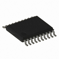
ATTINY167-15XD Atmel, ATTINY167-15XD Datasheet - Page 98

ATTINY167-15XD
Manufacturer Part Number
ATTINY167-15XD
Description
MCU AVR 16K FLASH 15MHZ 20-TSSOP
Manufacturer
Atmel
Series
AVR® ATtinyr
Datasheet
1.ATTINY167-15MD.pdf
(283 pages)
Specifications of ATTINY167-15XD
Core Processor
AVR
Core Size
8-Bit
Speed
16MHz
Connectivity
I²C, LIN, SPI, UART/USART, USI
Peripherals
Brown-out Detect/Reset, POR, PWM, Temp Sensor, WDT
Number Of I /o
16
Program Memory Size
16KB (8K x 16)
Program Memory Type
FLASH
Eeprom Size
512 x 8
Ram Size
512 x 8
Voltage - Supply (vcc/vdd)
2.7 V ~ 5.5 V
Data Converters
A/D 11x10b
Oscillator Type
Internal
Operating Temperature
-40°C ~ 150°C
Package / Case
20-TSSOP
Processor Series
ATTINY1x
Core
AVR8
Data Bus Width
8 bit
Data Ram Size
512 B
Maximum Clock Frequency
16 MHz
Maximum Operating Temperature
+ 85 C
Mounting Style
SMD/SMT
3rd Party Development Tools
EWAVR, EWAVR-BL
Development Tools By Supplier
ATAVRDRAGON, ATSTK500, ATSTK600, ATAVRISP2, ATAVRONEKIT
Minimum Operating Temperature
- 40 C
For Use With
ATSTK600-SOIC - STK600 SOCKET/ADAPTER FOR SOIC
Lead Free Status / RoHS Status
Lead free / RoHS Compliant
- Current page: 98 of 283
- Download datasheet (5Mb)
10.9
98
Asynchronous Operation of Timer/Counter0
ATtiny87/ATtiny167
Figure 10-11
Figure 10-11. Timer/Counter Timing Diagram, Clear Timer on Compare Match mode, with
When Timer/Counter0 operates asynchronously, some considerations must be taken.
• Warning: When switching between asynchronous and synchronous clocking of
• If an 32.768 kHz watch crystal is used, the CPU main clock frequency must be more than
• When writing to one of the registers TCNT0, OCR0A, or TCCR0A, the value is transferred
• When entering Power-save mode after having written to TCNT0, OCR0A, or TCCR0A, the
• If Timer/Counter0 is used to wake the device up from Power-save mode, precautions must
TCNTn
(clk
(CTC)
OCRnx
OCFnx
Timer/Counter0, the timer registers TCNT0, OCR0A, and TCCR0A might be corrupted. A
safe procedure for switching clock source is:
four times the Oscillator or external clock frequency.
to a temporary register, and latched after two positive edges on TOSC1. The user should
not write a new value before the contents of the temporary register have been transferred
to its destination. Each of the three mentioned registers have their individual temporary
register, which means that e.g. writing to TCNT0 does not disturb an OCR0A write in
progress. To detect that a transfer to the destination register has taken place, the
Asynchronous Status Register – ASSR has been implemented.
user must wait until the written register has been updated if Timer/Counter0 is used to
wake up the device. Otherwise, the MCU will enter sleep mode before the changes are
effective. This is particularly important if the Output Compare0 interrupt is used to wake up
the device, since the Output Compare function is disabled during writing to OCR0A or
TCNT0. If the write cycle is not finished, and the MCU enters sleep mode before the
OCR0UB bit returns to zero, the device will never receive a compare match interrupt, and
the MCU will not wake up.
be taken if the user wants to re-enter one of these modes: The interrupt logic needs one
clk
clk
I/O
I/O
Tn
a. Disable the Timer/Counter0 interrupts by clearing OCIE0A and TOIE0.
b. Select clock source by setting AS0 and EXCLK as appropriate.
c. Write new values to TCNT0, OCR0A, and TCCR0A.
d. To switch to asynchronous operation: Wait for TCN0UB, OCR0UB, and TCR0UB.
e. Clear the Timer/Counter0 interrupt flags.
f.
/8)
Enable interrupts, if needed.
shows the setting of OCF0A and the clearing of TCNT0 in CTC mode.
Prescaler (f
TOP - 1
clk_I/O
/8)
TOP
TOP
BOTTOM
BOTTOM + 1
7728G–AVR–06/10
Related parts for ATTINY167-15XD
Image
Part Number
Description
Manufacturer
Datasheet
Request
R

Part Number:
Description:
Manufacturer:
Atmel Corporation
Datasheet:

Part Number:
Description:
Manufacturer:
Atmel Corporation
Datasheet:

Part Number:
Description:
MCU AVR 16K FLASH 15MHZ 32-QFN
Manufacturer:
Atmel
Datasheet:

Part Number:
Description:
IC MCU AVR 16K FLASH 20TSSOP
Manufacturer:
Atmel
Datasheet:

Part Number:
Description:
MCU AVR 16K FLASH 15MHZ 32-QFN
Manufacturer:
Atmel
Datasheet:

Part Number:
Description:
MCU AVR 16K FLASH 15MHZ 20-SOIC
Manufacturer:
Atmel
Datasheet:

Part Number:
Description:
MCU AVR 16K FLASH 15MHZ 20-TSSOP
Manufacturer:
Atmel
Datasheet:

Part Number:
Description:
IC MCU AVR 16K FLASH 20SOIC
Manufacturer:
Atmel
Datasheet:


