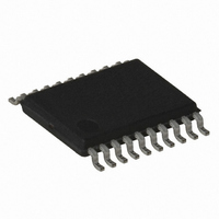
ATTINY167-15XD Atmel, ATTINY167-15XD Datasheet - Page 83

ATTINY167-15XD
Manufacturer Part Number
ATTINY167-15XD
Description
MCU AVR 16K FLASH 15MHZ 20-TSSOP
Manufacturer
Atmel
Series
AVR® ATtinyr
Datasheet
1.ATTINY167-15MD.pdf
(283 pages)
Specifications of ATTINY167-15XD
Core Processor
AVR
Core Size
8-Bit
Speed
16MHz
Connectivity
I²C, LIN, SPI, UART/USART, USI
Peripherals
Brown-out Detect/Reset, POR, PWM, Temp Sensor, WDT
Number Of I /o
16
Program Memory Size
16KB (8K x 16)
Program Memory Type
FLASH
Eeprom Size
512 x 8
Ram Size
512 x 8
Voltage - Supply (vcc/vdd)
2.7 V ~ 5.5 V
Data Converters
A/D 11x10b
Oscillator Type
Internal
Operating Temperature
-40°C ~ 150°C
Package / Case
20-TSSOP
Processor Series
ATTINY1x
Core
AVR8
Data Bus Width
8 bit
Data Ram Size
512 B
Maximum Clock Frequency
16 MHz
Maximum Operating Temperature
+ 85 C
Mounting Style
SMD/SMT
3rd Party Development Tools
EWAVR, EWAVR-BL
Development Tools By Supplier
ATAVRDRAGON, ATSTK500, ATSTK600, ATAVRISP2, ATAVRONEKIT
Minimum Operating Temperature
- 40 C
For Use With
ATSTK600-SOIC - STK600 SOCKET/ADAPTER FOR SOIC
Lead Free Status / RoHS Status
Lead free / RoHS Compliant
- Current page: 83 of 283
- Download datasheet (5Mb)
7728G–AVR–06/10
• PCINT10/OC1AV/USCK/SCL – Port B, Bit 2
• PCINT9/OC1BU/DO – Port B, Bit 1
• PCINT8/OC1AU/DI/SDA – Port B, Bit 0
PCINT10: Pin Change Interrupt, source 10.
OC1AV: Output Compare and PWM Output A-V for Timer/Counter1. The PB2 pin has to be
USCK: Three-wire Mode USI Clock Input.
SCL: Two-wire Mode USI Clock Input.
PCINT9: Pin Change Interrupt, source 9.
OC1BU: Output Compare and PWM Output B-U for Timer/Counter1. The PB1 pin has to be
DO: Three-wire Mode USI Data Output. Three-wire mode data output overrides PORTB1
IPCINT8: Pin Change Interrupt, source 8.
OC1AU: Output Compare and PWM Output A-U for Timer/Counter1. The PB0 pin has to be
DI: Three-wire Mode USI Data Input. USI Three-wire mode does not override normal port
SDA: Two-wire Mode Serial Interface (USI) Data Input / Output.
configured as an output (DDB2 set (one)) to serve this function. The OC1AV pin is
also the output pin for the PWM mode timer function (c.f. OC1AV bit of TCCR1D regis-
ter).
configured as an output (DDB1 set (one)) to serve this function. The OC1BU pin is
also the output pin for the PWM mode timer function (c.f. OC1BU bit of TCCR1D reg-
ister).
and it is driven to the port when the data direction bit DDB1 is set. PORTB1 still
enables the pull-up, if the direction is input and PORTB1 is set
configured as an output (DDB0 set (one)) to serve this function. The OC1AU pin is
also the output pin for the PWM mode timer function (c.f. OC1AU bit of TCCR1D regis-
ter).
functions, so pin must be configure as an input for DI function.
ATtiny87/ATtiny167
(
one
).
83
Related parts for ATTINY167-15XD
Image
Part Number
Description
Manufacturer
Datasheet
Request
R

Part Number:
Description:
Manufacturer:
Atmel Corporation
Datasheet:

Part Number:
Description:
Manufacturer:
Atmel Corporation
Datasheet:

Part Number:
Description:
MCU AVR 16K FLASH 15MHZ 32-QFN
Manufacturer:
Atmel
Datasheet:

Part Number:
Description:
IC MCU AVR 16K FLASH 20TSSOP
Manufacturer:
Atmel
Datasheet:

Part Number:
Description:
MCU AVR 16K FLASH 15MHZ 32-QFN
Manufacturer:
Atmel
Datasheet:

Part Number:
Description:
MCU AVR 16K FLASH 15MHZ 20-SOIC
Manufacturer:
Atmel
Datasheet:

Part Number:
Description:
MCU AVR 16K FLASH 15MHZ 20-TSSOP
Manufacturer:
Atmel
Datasheet:

Part Number:
Description:
IC MCU AVR 16K FLASH 20SOIC
Manufacturer:
Atmel
Datasheet:


