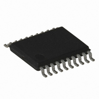
ATTINY167-15XD Atmel, ATTINY167-15XD Datasheet - Page 88

ATTINY167-15XD
Manufacturer Part Number
ATTINY167-15XD
Description
MCU AVR 16K FLASH 15MHZ 20-TSSOP
Manufacturer
Atmel
Series
AVR® ATtinyr
Datasheet
1.ATTINY167-15MD.pdf
(283 pages)
Specifications of ATTINY167-15XD
Core Processor
AVR
Core Size
8-Bit
Speed
16MHz
Connectivity
I²C, LIN, SPI, UART/USART, USI
Peripherals
Brown-out Detect/Reset, POR, PWM, Temp Sensor, WDT
Number Of I /o
16
Program Memory Size
16KB (8K x 16)
Program Memory Type
FLASH
Eeprom Size
512 x 8
Ram Size
512 x 8
Voltage - Supply (vcc/vdd)
2.7 V ~ 5.5 V
Data Converters
A/D 11x10b
Oscillator Type
Internal
Operating Temperature
-40°C ~ 150°C
Package / Case
20-TSSOP
Processor Series
ATTINY1x
Core
AVR8
Data Bus Width
8 bit
Data Ram Size
512 B
Maximum Clock Frequency
16 MHz
Maximum Operating Temperature
+ 85 C
Mounting Style
SMD/SMT
3rd Party Development Tools
EWAVR, EWAVR-BL
Development Tools By Supplier
ATAVRDRAGON, ATSTK500, ATSTK600, ATAVRISP2, ATAVRONEKIT
Minimum Operating Temperature
- 40 C
For Use With
ATSTK600-SOIC - STK600 SOCKET/ADAPTER FOR SOIC
Lead Free Status / RoHS Status
Lead free / RoHS Compliant
- Current page: 88 of 283
- Download datasheet (5Mb)
88
ATtiny87/ATtiny167
Figure 10-1. 8-bit Timer/Counter0 Block Diagram
The Timer/Counter (TCNT0) and Output Compare Register (OCR0A) are 8-bit registers. Inter-
rupt request (shorten as Int.Req.) signals are all visible in the Timer Interrupt Flag Register
(TIFR0). All interrupts are individually masked with the Timer Interrupt Mask Register
(TIMSK0). TIFR0 and TIMSK0 are not shown in the figure.
The Timer/Counter can be clocked internally, via the prescaler, or asynchronously clocked
from the XTAL1/2 pins, as detailed later in this section. The asynchronous operation is con-
trolled by the Asynchronous Status Register (ASSR). The Clock Select logic block controls
which clock source the Timer/Counter uses to increment (or decrement) its value. The
Timer/Counter is inactive when no clock source is selected. The output from the Clock Select
logic is referred to as the timer clock (clk
The double buffered Output Compare Register (OCR0A) is compared with the Timer/Counter
value at all times. The result of the compare can be used by the Waveform Generator to gen-
erate a PWM or variable frequency output on the Output Compare pin (OC0A).
Compare Unit” on page 90.
flag (OCF0A) which can be used to generate an Output Compare interrupt request.
Status flags
Timer/Counter
TCNTn
OCRnx
=
ASSRn
direction
count
clear
for details. The compare match event will also set the compare
BOTTOM
Synchronized Status flags
= 0
Control Logic
=
TCCRnx
T
TOP
asynchronous mode
0xFF
0).
select (ASn)
clk
Tn
Synchronization Unit
Prescaler
OCnx
(Int.Req.)
Generation
Waveform
Oscillator
OCnx
clk
7728G–AVR–06/10
TOVn
(Int.Req.)
clk
clk
See ”Output
ASY
I/O
I/O
XTAL1
XTAL2
Related parts for ATTINY167-15XD
Image
Part Number
Description
Manufacturer
Datasheet
Request
R

Part Number:
Description:
Manufacturer:
Atmel Corporation
Datasheet:

Part Number:
Description:
Manufacturer:
Atmel Corporation
Datasheet:

Part Number:
Description:
MCU AVR 16K FLASH 15MHZ 32-QFN
Manufacturer:
Atmel
Datasheet:

Part Number:
Description:
IC MCU AVR 16K FLASH 20TSSOP
Manufacturer:
Atmel
Datasheet:

Part Number:
Description:
MCU AVR 16K FLASH 15MHZ 32-QFN
Manufacturer:
Atmel
Datasheet:

Part Number:
Description:
MCU AVR 16K FLASH 15MHZ 20-SOIC
Manufacturer:
Atmel
Datasheet:

Part Number:
Description:
MCU AVR 16K FLASH 15MHZ 20-TSSOP
Manufacturer:
Atmel
Datasheet:

Part Number:
Description:
IC MCU AVR 16K FLASH 20SOIC
Manufacturer:
Atmel
Datasheet:


