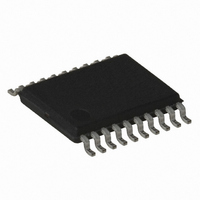
ATTINY167-15XD Atmel, ATTINY167-15XD Datasheet - Page 7

ATTINY167-15XD
Manufacturer Part Number
ATTINY167-15XD
Description
MCU AVR 16K FLASH 15MHZ 20-TSSOP
Manufacturer
Atmel
Series
AVR® ATtinyr
Datasheet
1.ATTINY167-15MD.pdf
(283 pages)
Specifications of ATTINY167-15XD
Core Processor
AVR
Core Size
8-Bit
Speed
16MHz
Connectivity
I²C, LIN, SPI, UART/USART, USI
Peripherals
Brown-out Detect/Reset, POR, PWM, Temp Sensor, WDT
Number Of I /o
16
Program Memory Size
16KB (8K x 16)
Program Memory Type
FLASH
Eeprom Size
512 x 8
Ram Size
512 x 8
Voltage - Supply (vcc/vdd)
2.7 V ~ 5.5 V
Data Converters
A/D 11x10b
Oscillator Type
Internal
Operating Temperature
-40°C ~ 150°C
Package / Case
20-TSSOP
Processor Series
ATTINY1x
Core
AVR8
Data Bus Width
8 bit
Data Ram Size
512 B
Maximum Clock Frequency
16 MHz
Maximum Operating Temperature
+ 85 C
Mounting Style
SMD/SMT
3rd Party Development Tools
EWAVR, EWAVR-BL
Development Tools By Supplier
ATAVRDRAGON, ATSTK500, ATSTK600, ATAVRISP2, ATAVRONEKIT
Minimum Operating Temperature
- 40 C
For Use With
ATSTK600-SOIC - STK600 SOCKET/ADAPTER FOR SOIC
Lead Free Status / RoHS Status
Lead free / RoHS Compliant
- Current page: 7 of 283
- Download datasheet (5Mb)
2. AVR CPU Core
2.1
7728G–AVR–06/10
Overview
This section discusses the AVR core architecture in general. The main function of the CPU
core is to ensure correct program execution. The CPU must therefore be able to access mem-
ories, perform calculations, control peripherals, and handle interrupts.
Figure 2-1.
In order to maximize performance and parallelism, the AVR uses a Harvard architecture – with
separate memories and buses for program and data. Instructions in the Program memory are
executed with a single level pipelining. While one instruction is being executed, the next
instruction is pre-fetched from the Program memory. This concept enables instructions to be
executed in every clock cycle. The Program memory is In-System Reprogrammable Flash
memory. The fast-access Register File contains 32 x 8-bit general purpose working registers
with a single clock cycle access time. This allows single-cycle Arithmetic Logic Unit (ALU)
operation. In a typical ALU operation, two operands are output from the Register File, the
operation is executed, and the result is stored back in the Register File – in one clock cycle.
Control Lines
Instruction
Instruction
Program
Memory
Decoder
Register
Flash
Block Diagram of the AVR Architecture
Program
Counter
and Control
EEPROM
Registrers
I/O Lines
Purpose
General
SRAM
Data Bus 8-bit
Status
32 x 8
Data
ALU
ATtiny87/ATtiny167
I/O Module1
Comparator
I/O Module 2
I/O Module n
Watchdog
Interrupt
Timer
A.D.C.
Analog
Unit
7
Related parts for ATTINY167-15XD
Image
Part Number
Description
Manufacturer
Datasheet
Request
R

Part Number:
Description:
Manufacturer:
Atmel Corporation
Datasheet:

Part Number:
Description:
Manufacturer:
Atmel Corporation
Datasheet:

Part Number:
Description:
MCU AVR 16K FLASH 15MHZ 32-QFN
Manufacturer:
Atmel
Datasheet:

Part Number:
Description:
IC MCU AVR 16K FLASH 20TSSOP
Manufacturer:
Atmel
Datasheet:

Part Number:
Description:
MCU AVR 16K FLASH 15MHZ 32-QFN
Manufacturer:
Atmel
Datasheet:

Part Number:
Description:
MCU AVR 16K FLASH 15MHZ 20-SOIC
Manufacturer:
Atmel
Datasheet:

Part Number:
Description:
MCU AVR 16K FLASH 15MHZ 20-TSSOP
Manufacturer:
Atmel
Datasheet:

Part Number:
Description:
IC MCU AVR 16K FLASH 20SOIC
Manufacturer:
Atmel
Datasheet:


