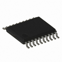
ATTINY167-15XD Atmel, ATTINY167-15XD Datasheet - Page 64

ATTINY167-15XD
Manufacturer Part Number
ATTINY167-15XD
Description
MCU AVR 16K FLASH 15MHZ 20-TSSOP
Manufacturer
Atmel
Series
AVR® ATtinyr
Datasheet
1.ATTINY167-15MD.pdf
(283 pages)
Specifications of ATTINY167-15XD
Core Processor
AVR
Core Size
8-Bit
Speed
16MHz
Connectivity
I²C, LIN, SPI, UART/USART, USI
Peripherals
Brown-out Detect/Reset, POR, PWM, Temp Sensor, WDT
Number Of I /o
16
Program Memory Size
16KB (8K x 16)
Program Memory Type
FLASH
Eeprom Size
512 x 8
Ram Size
512 x 8
Voltage - Supply (vcc/vdd)
2.7 V ~ 5.5 V
Data Converters
A/D 11x10b
Oscillator Type
Internal
Operating Temperature
-40°C ~ 150°C
Package / Case
20-TSSOP
Processor Series
ATTINY1x
Core
AVR8
Data Bus Width
8 bit
Data Ram Size
512 B
Maximum Clock Frequency
16 MHz
Maximum Operating Temperature
+ 85 C
Mounting Style
SMD/SMT
3rd Party Development Tools
EWAVR, EWAVR-BL
Development Tools By Supplier
ATAVRDRAGON, ATSTK500, ATSTK600, ATAVRISP2, ATAVRONEKIT
Minimum Operating Temperature
- 40 C
For Use With
ATSTK600-SOIC - STK600 SOCKET/ADAPTER FOR SOIC
Lead Free Status / RoHS Status
Lead free / RoHS Compliant
- Current page: 64 of 283
- Download datasheet (5Mb)
8.3.3
8.3.4
64
ATtiny87/ATtiny167
External Interrupt Flag Register – EIFR
Pin Change Interrupt Control Register – PCICR
• Bit 1 – INT1: External Interrupt Request 1 Enable
When the INT1 bit is set (one) and the I-bit in the Status Register (SREG) is set (one), the
external pin interrupt is enabled. The Interrupt Sense Control1 bits 1/0 (ISC11 and ISC10) in
the External Interrupt Control Register A (EICRA) define whether the external interrupt is acti-
vated on rising and/or falling edge of the INT1 pin or level sensed. Activity on the pin will cause
an interrupt request even if INT1 is configured as an output. The corresponding interrupt of
External Interrupt Request 1 is executed from the INT1 Interrupt Vector.
• Bit 0 – INT0: External Interrupt Request 0 Enable
When the INT0 bit is set (one) and the I-bit in the Status Register (SREG) is set (one), the
external pin interrupt is enabled. The Interrupt Sense Control0 bits 1/0 (ISC01 and ISC00) in
the External Interrupt Control Register A (EICRA) define whether the external interrupt is acti-
vated on rising and/or falling edge of the INT0 pin or level sensed. Activity on the pin will cause
an interrupt request even if INT0 is configured as an output. The corresponding interrupt of
External Interrupt Request 0 is executed from the INT0 Interrupt Vector.
• Bit 7, 2 – Res: Reserved Bits
These bits are unused bits in the ATtiny87/167, and will always read as zero.
• Bit 1 – INTF1: External Interrupt Flag 1
When an edge or logic change on the INT1 pin triggers an interrupt request, INTF1 becomes
set (one). If the I-bit in SREG and the INT1 bit in EIMSK are set (one), the MCU will jump to
the corresponding Interrupt Vector. The flag is cleared when the interrupt routine is executed.
Alternatively, the flag can be cleared by writing a logical one to it. This flag is always cleared
when INT1 is configured as a level interrupt.
• Bit 0 – INTF0: External Interrupt Flag 0
When an edge or logic change on the INT0 pin triggers an interrupt request, INTF0 becomes
set (one). If the I-bit in SREG and the INT0 bit in EIMSK are set (one), the MCU will jump to
the corresponding Interrupt Vector. The flag is cleared when the interrupt routine is executed.
Alternatively, the flag can be cleared by writing a logical one to it. This flag is always cleared
when INT0 is configured as a level interrupt.
• Bit 7, 2 – Res: Reserved Bits
These bits are unused bits in the ATtiny87/167, and will always read as zero.
Read/Write
Initial Value
Read/Write
Initial Value
Bit
Bit
R
R
7
–
0
7
–
0
R
R
6
–
0
6
–
0
R
R
5
–
0
5
–
0
R
R
4
–
0
4
–
0
R
R
3
–
0
3
–
0
R
R
2
–
0
2
–
0
PCIE1
INTF1
R/W
R/W
1
0
1
0
INTF0
PCIE0
R/W
R/W
0
0
0
0
7728G–AVR–06/10
PCICR
EIFR
Related parts for ATTINY167-15XD
Image
Part Number
Description
Manufacturer
Datasheet
Request
R

Part Number:
Description:
Manufacturer:
Atmel Corporation
Datasheet:

Part Number:
Description:
Manufacturer:
Atmel Corporation
Datasheet:

Part Number:
Description:
MCU AVR 16K FLASH 15MHZ 32-QFN
Manufacturer:
Atmel
Datasheet:

Part Number:
Description:
IC MCU AVR 16K FLASH 20TSSOP
Manufacturer:
Atmel
Datasheet:

Part Number:
Description:
MCU AVR 16K FLASH 15MHZ 32-QFN
Manufacturer:
Atmel
Datasheet:

Part Number:
Description:
MCU AVR 16K FLASH 15MHZ 20-SOIC
Manufacturer:
Atmel
Datasheet:

Part Number:
Description:
MCU AVR 16K FLASH 15MHZ 20-TSSOP
Manufacturer:
Atmel
Datasheet:

Part Number:
Description:
IC MCU AVR 16K FLASH 20SOIC
Manufacturer:
Atmel
Datasheet:


