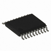
ATTINY167-15XD Atmel, ATTINY167-15XD Datasheet - Page 130

ATTINY167-15XD
Manufacturer Part Number
ATTINY167-15XD
Description
MCU AVR 16K FLASH 15MHZ 20-TSSOP
Manufacturer
Atmel
Series
AVR® ATtinyr
Datasheet
1.ATTINY167-15MD.pdf
(283 pages)
Specifications of ATTINY167-15XD
Core Processor
AVR
Core Size
8-Bit
Speed
16MHz
Connectivity
I²C, LIN, SPI, UART/USART, USI
Peripherals
Brown-out Detect/Reset, POR, PWM, Temp Sensor, WDT
Number Of I /o
16
Program Memory Size
16KB (8K x 16)
Program Memory Type
FLASH
Eeprom Size
512 x 8
Ram Size
512 x 8
Voltage - Supply (vcc/vdd)
2.7 V ~ 5.5 V
Data Converters
A/D 11x10b
Oscillator Type
Internal
Operating Temperature
-40°C ~ 150°C
Package / Case
20-TSSOP
Processor Series
ATTINY1x
Core
AVR8
Data Bus Width
8 bit
Data Ram Size
512 B
Maximum Clock Frequency
16 MHz
Maximum Operating Temperature
+ 85 C
Mounting Style
SMD/SMT
3rd Party Development Tools
EWAVR, EWAVR-BL
Development Tools By Supplier
ATAVRDRAGON, ATSTK500, ATSTK600, ATAVRISP2, ATAVRONEKIT
Minimum Operating Temperature
- 40 C
For Use With
ATSTK600-SOIC - STK600 SOCKET/ADAPTER FOR SOIC
Lead Free Status / RoHS Status
Lead free / RoHS Compliant
- Current page: 130 of 283
- Download datasheet (5Mb)
12.10 Timer/Counter Timing Diagrams
130
ATtiny87/ATtiny167
In phase and frequency correct PWM mode, the compare units allow generation of PWM
waveforms on the OC1A/B pins. Setting the COM1A/B1:0 bits to two will produce a
non-inverted PWM and an inverted PWM output can be generated by setting the COM1A/B1:0
to three (See
if the data direction for the port pin is set as output (DDR_OC1A/B) and OC1A/Bi is set. The
PWM waveform is generated by setting (or clearing) the OC1A/B Register at the compare
match between OCR1A/B and TCNT1 when the counter increments, and clearing (or setting)
the OC1A/B Register at compare match between OCR1A/B and TCNT1 when the counter
decrements. The PWM frequency for the output when using phase and frequency correct
PWM can be calculated by the following equation:
The N variable represents the prescaler divider (1, 8, 64, 256, or 1024).
The extreme values for the OCR1A/B Register represents special cases when generating a
PWM waveform output in the phase correct PWM mode. If the OCR1A/B is set equal to BOT-
TOM the output will be continuously low and if set equal to TOP the output will be set to high
for non-inverted PWM mode. For inverted PWM the output will have the opposite logic values.
The Timer/Counter is a synchronous design and the timer clock (clk
clock enable signal in the following figures. The figures include information on when interrupt
flags are set, and when the OCR1A/B Register is updated with the OCR1A/B buffer value
(only for modes utilizing double buffering).
of OCF1A/B.
Figure 12-11. Timer/Counter Timing Diagram, Setting of OCF1A/B, no Prescaling
Figure 12-12
TCNTn
OCRnx
OCFnx
(clk
clk
clk
I/O
shows the same timing data, but with the prescaler enabled.
Table on page
I/O
Tn
/1)
OCRnx - 1
133). The actual OC1A/B value will only be visible on the port pin
f
OCnxPFCPWM
OCRnx
Figure 12-11
OCRnx Value
=
---------------------------------
2
f
clk_I/O
N
OCRnx + 1
TOP
shows a timing diagram for the setting
T
1) is therefore shown as a
OCRnx + 2
7728G–AVR–06/10
Related parts for ATTINY167-15XD
Image
Part Number
Description
Manufacturer
Datasheet
Request
R

Part Number:
Description:
Manufacturer:
Atmel Corporation
Datasheet:

Part Number:
Description:
Manufacturer:
Atmel Corporation
Datasheet:

Part Number:
Description:
MCU AVR 16K FLASH 15MHZ 32-QFN
Manufacturer:
Atmel
Datasheet:

Part Number:
Description:
IC MCU AVR 16K FLASH 20TSSOP
Manufacturer:
Atmel
Datasheet:

Part Number:
Description:
MCU AVR 16K FLASH 15MHZ 32-QFN
Manufacturer:
Atmel
Datasheet:

Part Number:
Description:
MCU AVR 16K FLASH 15MHZ 20-SOIC
Manufacturer:
Atmel
Datasheet:

Part Number:
Description:
MCU AVR 16K FLASH 15MHZ 20-TSSOP
Manufacturer:
Atmel
Datasheet:

Part Number:
Description:
IC MCU AVR 16K FLASH 20SOIC
Manufacturer:
Atmel
Datasheet:


