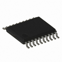
ATTINY167-15XD Atmel, ATTINY167-15XD Datasheet - Page 21

ATTINY167-15XD
Manufacturer Part Number
ATTINY167-15XD
Description
MCU AVR 16K FLASH 15MHZ 20-TSSOP
Manufacturer
Atmel
Series
AVR® ATtinyr
Datasheet
1.ATTINY167-15MD.pdf
(283 pages)
Specifications of ATTINY167-15XD
Core Processor
AVR
Core Size
8-Bit
Speed
16MHz
Connectivity
I²C, LIN, SPI, UART/USART, USI
Peripherals
Brown-out Detect/Reset, POR, PWM, Temp Sensor, WDT
Number Of I /o
16
Program Memory Size
16KB (8K x 16)
Program Memory Type
FLASH
Eeprom Size
512 x 8
Ram Size
512 x 8
Voltage - Supply (vcc/vdd)
2.7 V ~ 5.5 V
Data Converters
A/D 11x10b
Oscillator Type
Internal
Operating Temperature
-40°C ~ 150°C
Package / Case
20-TSSOP
Processor Series
ATTINY1x
Core
AVR8
Data Bus Width
8 bit
Data Ram Size
512 B
Maximum Clock Frequency
16 MHz
Maximum Operating Temperature
+ 85 C
Mounting Style
SMD/SMT
3rd Party Development Tools
EWAVR, EWAVR-BL
Development Tools By Supplier
ATAVRDRAGON, ATSTK500, ATSTK600, ATAVRISP2, ATAVRONEKIT
Minimum Operating Temperature
- 40 C
For Use With
ATSTK600-SOIC - STK600 SOCKET/ADAPTER FOR SOIC
Lead Free Status / RoHS Status
Lead free / RoHS Compliant
- Current page: 21 of 283
- Download datasheet (5Mb)
3.4
3.4.1
3.5
3.5.1
7728G–AVR–06/10
I/O Memory
Register Description
General Purpose I/O Registers
EEARH and EEARL – EEPROM Address Register
Keep the AVR RESET active (low) during periods of insufficient power supply voltage. This
can be done by enabling the internal Brown-out Detector (BOD). If the detection level of the
internal BOD does not match the needed detection level, an external low Vcc reset protection
circuit can be used. If a reset occurs while a write operation is in progress, the write operation
will be completed provided that the power supply voltage is sufficient.
The I/O space definition of the ATtiny87/167 is shown in
page
All ATtiny87/167 I/Os and peripherals are placed in the I/O space. All I/O locations may be
accessed by the LD/LDS/LDD and ST/STS/STD instructions, transferring data between the 32
general purpose working registers and the I/O space. I/O Registers within the address range
0x00 - 0x1F are directly bit-accessible using the SBI and CBI instructions. In these registers,
the value of single bits can be checked by using the SBIS and SBIC instructions. Refer to the
instruction set section for more details. When using the I/O specific commands IN and OUT,
the I/O addresses 0x00 - 0x3F must be used. When addressing I/O Registers as data space
using LD and ST instructions, 0x20 must be added to these addresses. The ATtiny87/167 is a
complex microcontroller with more peripheral units than can be supported within the 64 loca-
tion reserved in Opcode for the IN and OUT instructions. For the Extended I/O space from
0x60 - 0xFF in SRAM, only the ST/STS/STD and LD/LDS/LDD instructions can be used.
For compatibility with future devices, reserved bits should be written to zero if accessed.
Reserved I/O memory addresses should never be written.
Some of the Status Flags are cleared by writing a logical one to them. Note that, unlike most
other AVRs, the CBI and SBI instructions will only operate on the specified bit, and can there-
fore be used on registers containing such Status Flags. The CBI and SBI instructions work
with registers 0x00 to 0x1F only.
The I/O and Peripherals Control Registers are explained in later sections.
The ATtiny87/167 contains three General Purpose I/O Registers. These registers can be used
for storing any information, and they are particularly useful for storing global variables and Sta-
tus Flags.
The General Purpose I/O Registers within the address range 0x00 - 0x1F are directly
bit-accessible using the SBI, CBI, SBIS, and SBIC instructions.
Bit
Bit
Read/Write
Read/Write
Initial Value
Initial Value
268.
EEAR7
R/W
R
7
7
0
X
-
EEAR6
R/W
R
6
6
0
X
-
EEAR5
R/W
R
X
5
5
0
-
EEAR4
R/W
R
X
4
4
0
-
EEAR3
R/W
R
X
3
3
0
-
ATtiny87/ATtiny167
Section 25. “Register Summary” on
EEAR2
R/W
R
X
2
2
0
-
EEAR1
R/W
R
X
1
1
0
-
EEAR8
EEAR0
R/W
R/W
0
0
X
X
EEARH
EEARL
21
Related parts for ATTINY167-15XD
Image
Part Number
Description
Manufacturer
Datasheet
Request
R

Part Number:
Description:
Manufacturer:
Atmel Corporation
Datasheet:

Part Number:
Description:
Manufacturer:
Atmel Corporation
Datasheet:

Part Number:
Description:
MCU AVR 16K FLASH 15MHZ 32-QFN
Manufacturer:
Atmel
Datasheet:

Part Number:
Description:
IC MCU AVR 16K FLASH 20TSSOP
Manufacturer:
Atmel
Datasheet:

Part Number:
Description:
MCU AVR 16K FLASH 15MHZ 32-QFN
Manufacturer:
Atmel
Datasheet:

Part Number:
Description:
MCU AVR 16K FLASH 15MHZ 20-SOIC
Manufacturer:
Atmel
Datasheet:

Part Number:
Description:
MCU AVR 16K FLASH 15MHZ 20-TSSOP
Manufacturer:
Atmel
Datasheet:

Part Number:
Description:
IC MCU AVR 16K FLASH 20SOIC
Manufacturer:
Atmel
Datasheet:


