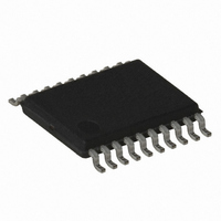
ATTINY167-15XD Atmel, ATTINY167-15XD Datasheet - Page 145

ATTINY167-15XD
Manufacturer Part Number
ATTINY167-15XD
Description
MCU AVR 16K FLASH 15MHZ 20-TSSOP
Manufacturer
Atmel
Series
AVR® ATtinyr
Datasheet
1.ATTINY167-15MD.pdf
(283 pages)
Specifications of ATTINY167-15XD
Core Processor
AVR
Core Size
8-Bit
Speed
16MHz
Connectivity
I²C, LIN, SPI, UART/USART, USI
Peripherals
Brown-out Detect/Reset, POR, PWM, Temp Sensor, WDT
Number Of I /o
16
Program Memory Size
16KB (8K x 16)
Program Memory Type
FLASH
Eeprom Size
512 x 8
Ram Size
512 x 8
Voltage - Supply (vcc/vdd)
2.7 V ~ 5.5 V
Data Converters
A/D 11x10b
Oscillator Type
Internal
Operating Temperature
-40°C ~ 150°C
Package / Case
20-TSSOP
Processor Series
ATTINY1x
Core
AVR8
Data Bus Width
8 bit
Data Ram Size
512 B
Maximum Clock Frequency
16 MHz
Maximum Operating Temperature
+ 85 C
Mounting Style
SMD/SMT
3rd Party Development Tools
EWAVR, EWAVR-BL
Development Tools By Supplier
ATAVRDRAGON, ATSTK500, ATSTK600, ATAVRISP2, ATAVRONEKIT
Minimum Operating Temperature
- 40 C
For Use With
ATSTK600-SOIC - STK600 SOCKET/ADAPTER FOR SOIC
Lead Free Status / RoHS Status
Lead free / RoHS Compliant
- Current page: 145 of 283
- Download datasheet (5Mb)
13.2
13.2.1
13.2.2
13.2.3
7728G–AVR–06/10
SS Pin Functionality
Slave Mode
Master Mode
SPI Control Register – SPCR
When the SPI is configured as a Slave, the Slave Select (SS) pin is always input. When SS is
held low, the SPI is activated, and MISO becomes an output if configured so by the user. All
other pins are inputs. When SS is driven high, all pins are inputs, and the SPI is passive, which
means that it will not receive incoming data. Note that the SPI logic will be reset once the SS
pin is driven high.
The SS pin is useful for packet/byte synchronization to keep the slave bit counter synchronous
with the master clock generator. When the SS pin is driven high, the SPI slave will immediately
reset the send and receive logic, and drop any partially received data in the Shift Register.
When the SPI is configured as a Master (MSTR in SPCR is set), the user can determine the
direction of the SS pin.
If SS is configured as an output, the pin is a general output pin which does not affect the SPI
system. Typically, the pin will be driving the SS pin of the SPI Slave.
If SS is configured as an input, it must be held high to ensure Master SPI operation. If the SS
pin is driven low by peripheral circuitry when the SPI is configured as a Master with the SS pin
defined as an input, the SPI system interprets this as another master selecting the SPI as a
slave and starting to send data to it. To avoid bus contention, the SPI system takes the follow-
ing actions:
Thus, when interrupt-driven SPI transmission is used in Master mode, and there exists a pos-
sibility that SS is driven low, the interrupt should always check that the MSTR bit is still set. If
the MSTR bit has been cleared by a slave select, it must be set by the user to re-enable SPI
Master mode.
• Bit 7 – SPIE: SPI Interrupt Enable
This bit causes the SPI interrupt to be executed if SPIF bit in the SPSR Register is set and if
the Global Interrupt Enable bit in SREG is set.
• Bit 6 – SPE: SPI Enable
When the SPE bit is written to one, the SPI is enabled. This bit must be set to enable any SPI
operations.
Bit
Read/Write
Initial Value
1. The MSTR bit in SPCR is cleared and the SPI system becomes a Slave. As a result
2. The SPIF flag in SPSR is set, and if the SPI interrupt is enabled, and the I-bit in
of the SPI becoming a Slave, the MOSI and SCK pins become inputs.
SREG is set, the interrupt routine will be executed.
SPIE
R/W
7
0
SPE
R/W
6
0
DORD
R/W
5
0
MSTR
R/W
4
0
CPOL
R/W
3
0
ATtiny87/ATtiny167
CPHA
R/W
2
0
SPR1
R/W
1
0
SPR0
R/W
0
0
SPCR
145
Related parts for ATTINY167-15XD
Image
Part Number
Description
Manufacturer
Datasheet
Request
R

Part Number:
Description:
Manufacturer:
Atmel Corporation
Datasheet:

Part Number:
Description:
Manufacturer:
Atmel Corporation
Datasheet:

Part Number:
Description:
MCU AVR 16K FLASH 15MHZ 32-QFN
Manufacturer:
Atmel
Datasheet:

Part Number:
Description:
IC MCU AVR 16K FLASH 20TSSOP
Manufacturer:
Atmel
Datasheet:

Part Number:
Description:
MCU AVR 16K FLASH 15MHZ 32-QFN
Manufacturer:
Atmel
Datasheet:

Part Number:
Description:
MCU AVR 16K FLASH 15MHZ 20-SOIC
Manufacturer:
Atmel
Datasheet:

Part Number:
Description:
MCU AVR 16K FLASH 15MHZ 20-TSSOP
Manufacturer:
Atmel
Datasheet:

Part Number:
Description:
IC MCU AVR 16K FLASH 20SOIC
Manufacturer:
Atmel
Datasheet:


