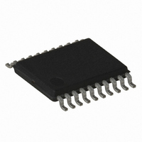
ATTINY167-15XD Atmel, ATTINY167-15XD Datasheet - Page 104

ATTINY167-15XD
Manufacturer Part Number
ATTINY167-15XD
Description
MCU AVR 16K FLASH 15MHZ 20-TSSOP
Manufacturer
Atmel
Series
AVR® ATtinyr
Datasheet
1.ATTINY167-15MD.pdf
(283 pages)
Specifications of ATTINY167-15XD
Core Processor
AVR
Core Size
8-Bit
Speed
16MHz
Connectivity
I²C, LIN, SPI, UART/USART, USI
Peripherals
Brown-out Detect/Reset, POR, PWM, Temp Sensor, WDT
Number Of I /o
16
Program Memory Size
16KB (8K x 16)
Program Memory Type
FLASH
Eeprom Size
512 x 8
Ram Size
512 x 8
Voltage - Supply (vcc/vdd)
2.7 V ~ 5.5 V
Data Converters
A/D 11x10b
Oscillator Type
Internal
Operating Temperature
-40°C ~ 150°C
Package / Case
20-TSSOP
Processor Series
ATTINY1x
Core
AVR8
Data Bus Width
8 bit
Data Ram Size
512 B
Maximum Clock Frequency
16 MHz
Maximum Operating Temperature
+ 85 C
Mounting Style
SMD/SMT
3rd Party Development Tools
EWAVR, EWAVR-BL
Development Tools By Supplier
ATAVRDRAGON, ATSTK500, ATSTK600, ATAVRISP2, ATAVRONEKIT
Minimum Operating Temperature
- 40 C
For Use With
ATSTK600-SOIC - STK600 SOCKET/ADAPTER FOR SOIC
Lead Free Status / RoHS Status
Lead free / RoHS Compliant
- Current page: 104 of 283
- Download datasheet (5Mb)
• Bit 5 – AS0: Asynchronous Timer/Counter0
When AS0 is written to zero, Timer/Counter0 is clocked from the I/O clock, clkI/O and the
Timer/Counter0 acts as a synchronous peripheral.
When AS0 is written to one, Timer/Counter0 is clocked from the low-frequency crystal oscilla-
tor
(See ”Low-frequency Crystal Oscillator” on page
29.) or from external clock on XTAL1 pin
(See ”External Clock” on page
30.) depending on EXCLK setting. When the value of AS0 is
changed, the contents of TCNT0, OCR0A, and TCCR0A might be corrupted.
AS0 also acts as a flag: Timer/Counter0 is clocked from the low-frequency crystal or from
external clock ONLY IF the calibrated internal RC oscillator or the internal watchdog oscillator
is used to drive the system clock. After setting AS0, if the switching is available, AS0 remains
to 1, else it is forced to 0.
• Bit 4 – TCN0UB: Timer/Counter0 Update Busy
When Timer/Counter0 operates asynchronously and TCNT0 is written, this bit becomes set.
When TCNT0 has been updated from the temporary storage register, this bit is cleared by
hardware. A logical zero in this bit indicates that TCNT0 is ready to be updated with a new
value.
• Bit 3 – OCR0AUB: Output Compare 0 Register A Update Busy
When Timer/Counter0 operates asynchronously and OCR0A is written, this bit becomes set.
When OCR0A has been updated from the temporary storage register, this bit is cleared by
hardware. A logical zero in this bit indicates that OCR0A is ready to be updated with a new
value.
• Bit 2 – Res: Reserved Bit
This bit is reserved in the ATtiny87/167 and will always read as zero.
• Bit 1 – TCR0AUB: Timer/Counter0 Control Register A Update Busy
When Timer/Counter0 operates asynchronously and TCCR0A is written, this bit becomes set.
When TCCR0A has been updated from the temporary storage register, this bit is cleared by
hardware. A logical zero in this bit indicates that TCCR0A is ready to be updated with a new
value.
• Bit 0 – TCR0BUB: Timer/Counter0 Control Register B Update Busy
When Timer/Counter0 operates asynchronously and TCCR0B is written, this bit becomes set.
When TCCR0B has been updated from the temporary storage register, this bit is cleared by
hardware. A logical zero in this bit indicates that TCCR0B is ready to be updated with a new
value.
If a write is performed to any of the four Timer/Counter0 Registers while its update busy flag is
set, the updated value might get corrupted and cause an unintentional interrupt to occur.
The mechanisms for reading TCNT0, OCR0A, TCCR0A and TCCR0B are different. When
reading TCNT0, the actual timer value is read. When reading OCR0A, TCCR0A or TCCR0B
the value in the temporary storage register is read.
ATtiny87/ATtiny167
104
7728G–AVR–06/10
Related parts for ATTINY167-15XD
Image
Part Number
Description
Manufacturer
Datasheet
Request
R

Part Number:
Description:
Manufacturer:
Atmel Corporation
Datasheet:

Part Number:
Description:
Manufacturer:
Atmel Corporation
Datasheet:

Part Number:
Description:
MCU AVR 16K FLASH 15MHZ 32-QFN
Manufacturer:
Atmel
Datasheet:

Part Number:
Description:
IC MCU AVR 16K FLASH 20TSSOP
Manufacturer:
Atmel
Datasheet:

Part Number:
Description:
MCU AVR 16K FLASH 15MHZ 32-QFN
Manufacturer:
Atmel
Datasheet:

Part Number:
Description:
MCU AVR 16K FLASH 15MHZ 20-SOIC
Manufacturer:
Atmel
Datasheet:

Part Number:
Description:
MCU AVR 16K FLASH 15MHZ 20-TSSOP
Manufacturer:
Atmel
Datasheet:

Part Number:
Description:
IC MCU AVR 16K FLASH 20SOIC
Manufacturer:
Atmel
Datasheet:


