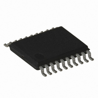
ATTINY167-15XD Atmel, ATTINY167-15XD Datasheet - Page 112

ATTINY167-15XD
Manufacturer Part Number
ATTINY167-15XD
Description
MCU AVR 16K FLASH 15MHZ 20-TSSOP
Manufacturer
Atmel
Series
AVR® ATtinyr
Datasheet
1.ATTINY167-15MD.pdf
(283 pages)
Specifications of ATTINY167-15XD
Core Processor
AVR
Core Size
8-Bit
Speed
16MHz
Connectivity
I²C, LIN, SPI, UART/USART, USI
Peripherals
Brown-out Detect/Reset, POR, PWM, Temp Sensor, WDT
Number Of I /o
16
Program Memory Size
16KB (8K x 16)
Program Memory Type
FLASH
Eeprom Size
512 x 8
Ram Size
512 x 8
Voltage - Supply (vcc/vdd)
2.7 V ~ 5.5 V
Data Converters
A/D 11x10b
Oscillator Type
Internal
Operating Temperature
-40°C ~ 150°C
Package / Case
20-TSSOP
Processor Series
ATTINY1x
Core
AVR8
Data Bus Width
8 bit
Data Ram Size
512 B
Maximum Clock Frequency
16 MHz
Maximum Operating Temperature
+ 85 C
Mounting Style
SMD/SMT
3rd Party Development Tools
EWAVR, EWAVR-BL
Development Tools By Supplier
ATAVRDRAGON, ATSTK500, ATSTK600, ATAVRISP2, ATAVRONEKIT
Minimum Operating Temperature
- 40 C
For Use With
ATSTK600-SOIC - STK600 SOCKET/ADAPTER FOR SOIC
Lead Free Status / RoHS Status
Lead free / RoHS Compliant
- Current page: 112 of 283
- Download datasheet (5Mb)
12.2.2
12.3
112
Accessing 16-bit Registers
ATtiny87/ATtiny167
Definitions
The Timer/Counter can be clocked internally, via the prescaler, or by an external clock source
on the Tn pin. The Clock Select logic block controls which clock source and edge the
Timer/Counter uses to increment (or decrement) its value. The Timer/Counter is inactive when
no clock source is selected. The output from the Clock Select logic is referred to as the timer
clock (clk
The double buffered Output Compare Registers (OCR1A/B) are compared with the
Timer/Counter value at all time. The result of the compare can be used by the Waveform Gen-
erator to generate a PWM or variable frequency output on the Output Compare pins
”Output Compare Units” on page
Match Flag (OCF1A/B) which can be used to generate an Output Compare interrupt request.
The Input Capture Register can capture the Timer/Counter value at a given external (edge
triggered) event on either the Input Capture pin (ICP1) or on the Analog Comparator pins
”AnaComp - Analog Comparator” on page
ing unit (Noise Canceler) for reducing the chance of capturing noise spikes.
The TOP value, or maximum Timer/Counter value, can in some modes of operation be
defined by either the OCR1A Register, the ICR1 Register, or by a set of fixed values. When
using OCR1A as TOP value in a PWM mode, the OCR1A Register can not be used for gener-
ating a PWM output. However, the TOP value will in this case be double buffered allowing the
TOP value to be changed in run time. If a fixed TOP value is required, the ICR1 Register can
be used as an alternative, freeing the OCR1A to be used as PWM output.
The following definitions are used extensively throughout the section:
The TCNT1, OCR1A/B, and ICR1 are 16-bit registers that can be accessed by the AVR CPU
via the 8-bit data bus. The 16-bit register must be byte accessed using two read or write oper-
ations. Each 16-bit timer has a single 8-bit register for temporary storing of the high byte of the
16-bit access. The same temporary register is shared between all 16-bit registers within each
16-bit timer. Accessing the low byte triggers the 16-bit read or write operation. When the low
byte of a 16-bit register is written by the CPU, the high byte stored in the temporary register,
and the low byte written are both copied into the 16-bit register in the same clock cycle. When
the low byte of a 16-bit register is read by the CPU, the high byte of the 16-bit register is cop-
ied into the temporary register in the same clock cycle as the low byte is read.
Not all 16-bit accesses uses the temporary register for the high byte. Reading the OCR1A/B
16-bit registers does not involve using the temporary register.
To do a 16-bit write, the high byte must be written before the low byte. For a 16-bit read, the
low byte must be read before the high byte.
BOTTOM
MAX
TOP
T
n
).
The counter reaches the BOTTOM when it becomes 0x0000.
The counter reaches its MAXimum when it becomes 0xFFFF (decimal 65,535).
The counter reaches the TOP when it becomes equal to the highest value in
the count sequence. The TOP value can be assigned to be one of the fixed val-
ues: 0x00FF, 0x01FF, or 0x03FF, or to the value stored in the OCR1A or ICR1
Register. The assignment is dependent of the mode of operation.
119.. The compare match event will also set the Compare
211.). The Input Capture unit includes a digital filter-
7728G–AVR–06/10
(See
See
Related parts for ATTINY167-15XD
Image
Part Number
Description
Manufacturer
Datasheet
Request
R

Part Number:
Description:
Manufacturer:
Atmel Corporation
Datasheet:

Part Number:
Description:
Manufacturer:
Atmel Corporation
Datasheet:

Part Number:
Description:
MCU AVR 16K FLASH 15MHZ 32-QFN
Manufacturer:
Atmel
Datasheet:

Part Number:
Description:
IC MCU AVR 16K FLASH 20TSSOP
Manufacturer:
Atmel
Datasheet:

Part Number:
Description:
MCU AVR 16K FLASH 15MHZ 32-QFN
Manufacturer:
Atmel
Datasheet:

Part Number:
Description:
MCU AVR 16K FLASH 15MHZ 20-SOIC
Manufacturer:
Atmel
Datasheet:

Part Number:
Description:
MCU AVR 16K FLASH 15MHZ 20-TSSOP
Manufacturer:
Atmel
Datasheet:

Part Number:
Description:
IC MCU AVR 16K FLASH 20SOIC
Manufacturer:
Atmel
Datasheet:


