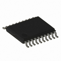
ATTINY167-15XD Atmel, ATTINY167-15XD Datasheet - Page 150

ATTINY167-15XD
Manufacturer Part Number
ATTINY167-15XD
Description
MCU AVR 16K FLASH 15MHZ 20-TSSOP
Manufacturer
Atmel
Series
AVR® ATtinyr
Datasheet
1.ATTINY167-15MD.pdf
(283 pages)
Specifications of ATTINY167-15XD
Core Processor
AVR
Core Size
8-Bit
Speed
16MHz
Connectivity
I²C, LIN, SPI, UART/USART, USI
Peripherals
Brown-out Detect/Reset, POR, PWM, Temp Sensor, WDT
Number Of I /o
16
Program Memory Size
16KB (8K x 16)
Program Memory Type
FLASH
Eeprom Size
512 x 8
Ram Size
512 x 8
Voltage - Supply (vcc/vdd)
2.7 V ~ 5.5 V
Data Converters
A/D 11x10b
Oscillator Type
Internal
Operating Temperature
-40°C ~ 150°C
Package / Case
20-TSSOP
Processor Series
ATTINY1x
Core
AVR8
Data Bus Width
8 bit
Data Ram Size
512 B
Maximum Clock Frequency
16 MHz
Maximum Operating Temperature
+ 85 C
Mounting Style
SMD/SMT
3rd Party Development Tools
EWAVR, EWAVR-BL
Development Tools By Supplier
ATAVRDRAGON, ATSTK500, ATSTK600, ATAVRISP2, ATAVRONEKIT
Minimum Operating Temperature
- 40 C
For Use With
ATSTK600-SOIC - STK600 SOCKET/ADAPTER FOR SOIC
Lead Free Status / RoHS Status
Lead free / RoHS Compliant
- Current page: 150 of 283
- Download datasheet (5Mb)
14.3
14.3.1
150
Functional Descriptions
ATtiny87/ATtiny167
Three-wire Mode
A transparent latch is inserted between the USI Data Register Output and output pin, which
delays the change of data output to the opposite clock edge of the data input sampling. The
serial input is always sampled from the Data Input (DI) pin independent of the configuration.
The 4-bit counter can be both read and written via the data bus, and can generate an overflow
interrupt. Both the USI Data Register and the counter are clocked simultaneously by the same
clock source. This allows the counter to count the number of bits received or transmitted and
generate an interrupt when the transfer is complete. Note that when an external clock source
is selected the counter counts both clock edges. In this case the counter counts the number of
edges, and not the number of bits. The clock can be selected from three different sources: The
USCK pin, Timer/Counter0 Compare Match or from software.
The Two-wire clock control unit can generate an interrupt when a start condition is detected on
the Two-wire bus. It can also generate wait states by holding the clock pin low after a start
condition is detected, or after the counter overflows.
The USI Three-wire mode is compliant to the Serial Peripheral Interface (SPI) mode 0 and 1,
but does not have the slave select (SS) pin functionality. However, this feature can be imple-
mented in software if necessary. Pin names used by this mode are: DI, DO, and USCK.
Figure 14-2. Three-wire Mode Operation, Simplified Diagram
Figure 14-2
Slave. The two USI Data Register are interconnected in such way that after eight USCK
clocks, the data in each register are interchanged. The same clock also increments the USI’s
4-bit counter. The Counter Overflow (interrupt) Flag, or USIOIF, can therefore be used to
determine when a transfer is completed.
SLAVE
MASTER
Bit7
Bit7
Bit6
Bit6
shows two USI units operating in Three-wire mode, one as Master and one as
Bit5
Bit5
Bit4
Bit4
Bit3
Bit3
Bit2
Bit2
Bit1
Bit1
Bit0
Bit0
PORTxn
USCK
USCK
DO
DO
DI
DI
7728G–AVR–06/10
Related parts for ATTINY167-15XD
Image
Part Number
Description
Manufacturer
Datasheet
Request
R

Part Number:
Description:
Manufacturer:
Atmel Corporation
Datasheet:

Part Number:
Description:
Manufacturer:
Atmel Corporation
Datasheet:

Part Number:
Description:
MCU AVR 16K FLASH 15MHZ 32-QFN
Manufacturer:
Atmel
Datasheet:

Part Number:
Description:
IC MCU AVR 16K FLASH 20TSSOP
Manufacturer:
Atmel
Datasheet:

Part Number:
Description:
MCU AVR 16K FLASH 15MHZ 32-QFN
Manufacturer:
Atmel
Datasheet:

Part Number:
Description:
MCU AVR 16K FLASH 15MHZ 20-SOIC
Manufacturer:
Atmel
Datasheet:

Part Number:
Description:
MCU AVR 16K FLASH 15MHZ 20-TSSOP
Manufacturer:
Atmel
Datasheet:

Part Number:
Description:
IC MCU AVR 16K FLASH 20SOIC
Manufacturer:
Atmel
Datasheet:


