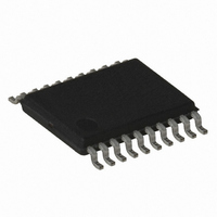
ATTINY167-15XD Atmel, ATTINY167-15XD Datasheet - Page 40

ATTINY167-15XD
Manufacturer Part Number
ATTINY167-15XD
Description
MCU AVR 16K FLASH 15MHZ 20-TSSOP
Manufacturer
Atmel
Series
AVR® ATtinyr
Datasheet
1.ATTINY167-15MD.pdf
(283 pages)
Specifications of ATTINY167-15XD
Core Processor
AVR
Core Size
8-Bit
Speed
16MHz
Connectivity
I²C, LIN, SPI, UART/USART, USI
Peripherals
Brown-out Detect/Reset, POR, PWM, Temp Sensor, WDT
Number Of I /o
16
Program Memory Size
16KB (8K x 16)
Program Memory Type
FLASH
Eeprom Size
512 x 8
Ram Size
512 x 8
Voltage - Supply (vcc/vdd)
2.7 V ~ 5.5 V
Data Converters
A/D 11x10b
Oscillator Type
Internal
Operating Temperature
-40°C ~ 150°C
Package / Case
20-TSSOP
Processor Series
ATTINY1x
Core
AVR8
Data Bus Width
8 bit
Data Ram Size
512 B
Maximum Clock Frequency
16 MHz
Maximum Operating Temperature
+ 85 C
Mounting Style
SMD/SMT
3rd Party Development Tools
EWAVR, EWAVR-BL
Development Tools By Supplier
ATAVRDRAGON, ATSTK500, ATSTK600, ATAVRISP2, ATAVRONEKIT
Minimum Operating Temperature
- 40 C
For Use With
ATSTK600-SOIC - STK600 SOCKET/ADAPTER FOR SOIC
Lead Free Status / RoHS Status
Lead free / RoHS Compliant
- Current page: 40 of 283
- Download datasheet (5Mb)
4.5.4
40
ATtiny87/ATtiny167
CLKSELR - Clock Selection Register
start-up time, the clock frequency and, of course, if the clock is alive. The user’s code has to
differentiate between ‘no_clock_signal’ and ‘clock_signal_not_yet_available’ condition.
• Bits 3:0 – CLKC3:0: Clock Control Bits 3 - 0
These bits define the command to provide to the ‘Clock Switch’ module. The special write pro-
cedure must be followed to change the CLKC3..0 bits
Change Enable” on page
Interrupts should be disabled when setting CLKCSR register in order not to disturb the
procedure.
Table 4-11.
• Bit 7– Res: Reserved Bit
This bit is reserved bit in the ATtiny87/167 and will always read as zero.
• Bit 6 – COUT: Clock Out
The COUT bit is initialized with ~(CKOUT) Fuse bit.
The COUT bit is only used in case of ‘CKOUT’ command. Refer to
Buffer” on page 31
In case of ‘Recover System Clock Source’ command, COUT it is not affected (no recovering of
this setting).
Bit
Read/Write
Initial Value
Clock Command
No command
Disable clock source
Enable clock source
Request for clock
Clock source switch
Recover system clock source code
Enable watchdog in automatic reload mode
CKOUT command
No command
1. Write the Clock Control Change Enable (CLKCCE) bit to one and all other bits in
2. Within 4 cycles, write the desired value to CLKCSR register while clearing CLKCCE
CLKCSR to zero.
bit.
Clock command list.
R
7
0
-
availability
for using.
~ (CKOUT)
COUT
R/W
fuse
6
39.).
CSUT1
R/W
5
SUT1..0
fuses
CSUT0
R/W
4
CSEL3
R/W
3
(See ”Bit 7 – CLKCCE: Clock Control
CSEL2
R/W
2
CKSEL3..0
fuses
Section 4.2.7 “Clock Output
CSEL1
R/W
1
CSEL0
R/W
0
CLKC3..0
7728G–AVR–06/10
1xxx
0000
0001
0010
0011
0100
0101
0110
0111
CLKSELR
b
b
b
b
b
b
b
b
b
Related parts for ATTINY167-15XD
Image
Part Number
Description
Manufacturer
Datasheet
Request
R

Part Number:
Description:
Manufacturer:
Atmel Corporation
Datasheet:

Part Number:
Description:
Manufacturer:
Atmel Corporation
Datasheet:

Part Number:
Description:
MCU AVR 16K FLASH 15MHZ 32-QFN
Manufacturer:
Atmel
Datasheet:

Part Number:
Description:
IC MCU AVR 16K FLASH 20TSSOP
Manufacturer:
Atmel
Datasheet:

Part Number:
Description:
MCU AVR 16K FLASH 15MHZ 32-QFN
Manufacturer:
Atmel
Datasheet:

Part Number:
Description:
MCU AVR 16K FLASH 15MHZ 20-SOIC
Manufacturer:
Atmel
Datasheet:

Part Number:
Description:
MCU AVR 16K FLASH 15MHZ 20-TSSOP
Manufacturer:
Atmel
Datasheet:

Part Number:
Description:
IC MCU AVR 16K FLASH 20SOIC
Manufacturer:
Atmel
Datasheet:


