OM13006,598 NXP Semiconductors, OM13006,598 Datasheet - Page 299
OM13006,598
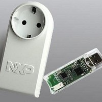
Manufacturer Part Number
OM13006,598
Description
BOARD EVAL EM773 METER EU PLUG
Manufacturer
NXP Semiconductors
Type
Other Power Managementr
Specifications of OM13006,598
Design Resources
Plug Meter Schematics, Gerber Files USB Dongle Schematics, Gerber Files
Main Purpose
Power Management, Energy/Power Meter
Embedded
Yes, MCU, 32-Bit
Utilized Ic / Part
EM773FHN33,551
Interface Type
USB
Maximum Operating Temperature
+ 150 C
Operating Supply Voltage
1.8 V to 3.6 V
Product
Power Management Development Tools
Lead Free Status / RoHS Status
Lead free / RoHS Compliant
Primary Attributes
-
Secondary Attributes
-
Lead Free Status / Rohs Status
Lead free / RoHS Compliant
For Use With/related Products
EM773, OL2381
Other names
568-6681


NXP Semiconductors
Table 161: Timer Control Register (TMR32B0TCR - address
Table 162: Match Control Register (TMR32B0MCR -
Table 163: Capture Control Register (TMR32B0CCR -
Table 164: External Match Register (TMR32B0EMR -
Table 165. External match control . . . . . . . . . . . . . . . . . .173
Table 166: Count Control Register (TMR32B0CTCR -
Table 167: PWM Control Register (TMR32B0PWMC -
Table 168. Register overview: Watchdog timer (base
Table 169. Watchdog Mode register (WDMOD - address
Table 170. Watchdog operating modes selection . . . . . .181
Table 171. Watchdog Constant register (WDTC - address
Table 172. Watchdog Feed register (WDFEED - address
Table 173. Watchdog Timer Value register (WDTV - address
Table 174. Register overview: SysTick timer (base address
Table 175. System Timer Reload value register (SYST_RVR
Table 176. System Timer Current value register (SYST_CVR
Table 177. System Timer Calibration value register
Table 178. Serial Wire Debug pin description . . . . . . . . .188
Table 179. Metrology Engine configuration parameters .192
Table 180. Metrology result class structure . . . . . . . . . . .200
Table 181. Flash sector configuration . . . . . . . . . . . . . . .204
Table 182. Code Read Protection options . . . . . . . . . . . .205
Table 183. Code Read Protection hardware/software
Table 184. ISP commands allowed for different CRP levels .
Table 185. UART ISP command summary . . . . . . . . . . .208
Table 186. UART ISP Unlock command . . . . . . . . . . . . .209
Table 187. UART ISP Set Baud Rate command . . . . . . .209
Table 188. UART ISP Echo command . . . . . . . . . . . . . .209
Table 189. UART ISP Write to RAM command . . . . . . . .210
Table 190. UART ISP Read Memory command . . . . . . .210
Table 191. UART ISP Prepare sector(s) for write operation
Table 192. UART ISP Copy command . . . . . . . . . . . . . . 211
Table 193. UART ISP Go command . . . . . . . . . . . . . . . .212
Table 194. UART ISP Erase sector command . . . . . . . .212
UM10415
User manual
0x4001 4004 and TMR32B1TCR - address
0x4001 8004) bit description . . . . . . . . . . . . .170
address 0x4001 4014 and TMR32B1MCR -
address 0x4001 8014) bit description. . . . . . .171
address 0x4001 4028) bit description. . . . . . .172
address 0x4001 403C and TMR32B1EMR -
address0x4001 803C) bit description . . . . . . .173
address 0x4001 4070 and TMR32B1TCR -
address 0x4001 8070) bit description . . . . . .174
0x4001 4074 and TMR32B1PWMC - 0x4001
8074) bit description . . . . . . . . . . . . . . . . . . . .175
address 0x4000 4000) . . . . . . . . . . . . . . . . . .180
0x4000 4000) bit description . . . . . . . . . . . . .180
0x4000 4004) bit description . . . . . . . . . . . . .181
0x4000 4008) bit description . . . . . . . . . . . . .181
0x4000 000C) bit description . . . . . . . . . . . . .182
0xE000 E000) . . . . . . . . . . . . . . . . . . . . . . . . .184
- 0xE000 E014) bit description . . . . . . . . . . . .185
- 0xE000 E018) bit description . . . . . . . . . . . .185
(SYST_CALIB - 0xE000 E01C) bit description . . .
185
interaction . . . . . . . . . . . . . . . . . . . . . . . . . . .205
206
command . . . . . . . . . . . . . . . . . . . . . . . . . . . . 211
All information provided in this document is subject to legal disclaimers.
Rev. 1 — 10 September 2010
Table 195. UART ISP Blank check sector command . . . 213
Table 196. UART ISP Read Part Identification command213
Table 197. EM773 part identification numbers . . . . . . . . 213
Table 198. UART ISP Read Boot Code version number
Table 199. UART ISP Compare command . . . . . . . . . . . 214
Table 200. UART ISP ReadUID command . . . . . . . . . . . 214
Table 201. UART ISP Return Codes Summary . . . . . . . 214
Table 202. IAP Command Summary . . . . . . . . . . . . . . . 216
Table 203. IAP Prepare sector(s) for write operation
Table 204. IAP Copy RAM to flash command. . . . . . . . . 218
Table 205. IAP Erase Sector(s) command . . . . . . . . . . . 218
Table 206. IAP Blank check sector(s) command . . . . . . 219
Table 207. IAP Read Part Identification command . . . . . 219
Table 208. IAP Read Boot Code version number command
Table 209. IAP Compare command . . . . . . . . . . . . . . . . 220
Table 210. IAP Reinvoke ISP . . . . . . . . . . . . . . . . . . . . . 220
Table 211. IAP ReadUID command . . . . . . . . . . . . . . . . 220
Table 212. IAP Status Codes Summary . . . . . . . . . . . . . 221
Table 213. Memory mapping in debug mode . . . . . . . . . 221
Table 214. Flash configuration register (FLASHCFG,
Table 215. Serial Wire Debug pin description. . . . . . . . . 223
Table 216. Summary of processor mode and stack use
Table 217. Core register set summary . . . . . . . . . . . . . . 228
Table 218. PSR register combinations . . . . . . . . . . . . . . 229
Table 219. APSR bit assignments . . . . . . . . . . . . . . . . . 230
Table 220. IPSR bit assignments . . . . . . . . . . . . . . . . . . 230
Table 221. EPSR bit assignments . . . . . . . . . . . . . . . . . 231
Table 222. PRIMASK register bit assignments . . . . . . . . 231
Table 223. CONTROL register bit assignments . . . . . . . 232
Table 224. Memory access behavior . . . . . . . . . . . . . . . 236
Table 225. Properties of different exception types . . . . . 238
Table 226. Exception return behavior . . . . . . . . . . . . . . . 243
Table 227. Cortex-M0 instructions . . . . . . . . . . . . . . . . . 246
Table 228. CMSIS intrinsic functions to generate some
Table 229. insic functions to access the special registers . .
Table 230. Condition code suffixes . . . . . . . . . . . . . . . . . 253
Table 231. Access instructions . . . . . . . . . . . . . . . . . . . 253
Table 232. Data processing instructions . . . . . . . . . . . . . 259
Table 233. ADC, ADD, RSB, SBC and SUB operand
Table 234. Branch and control instructions. . . . . . . . . . . 268
Table 235. Branch ranges. . . . . . . . . . . . . . . . . . . . . . . . 269
Table 236. Miscellaneous instructions . . . . . . . . . . . . . . 270
Table 237. Core peripheral register regions . . . . . . . . . . 277
Table 238. NVIC register summary. . . . . . . . . . . . . . . . . 278
Table 239. CMISIS access NVIC functions . . . . . . . . . . 278
Table 240. ISER bit assignments . . . . . . . . . . . . . . . . . . 279
Table 241. ICER bit assignments . . . . . . . . . . . . . . . . . . 279
Table 242. ISPR bit assignments . . . . . . . . . . . . . . . . . . 279
Table 243. ICPR bit assignments . . . . . . . . . . . . . . . . . . 280
Table 244. IPR bit assignments . . . . . . . . . . . . . . . . . . . 280
Chapter 21: EM773 Supplementary information
command . . . . . . . . . . . . . . . . . . . . . . . . . . . . 213
command . . . . . . . . . . . . . . . . . . . . . . . . . . . . 217
219
address 0x4003 C010) bit description . . . . . . 222
options . . . . . . . . . . . . . . . . . . . . . . . . . . . . . . 227
Cortex-M0 instructions . . . . . . . . . . . . . . . . . . 247
248
restrictions . . . . . . . . . . . . . . . . . . . . . . . . . . . 261
UM10415
© NXP B.V. 2010. All rights reserved.
299 of 310
Related parts for OM13006,598
Image
Part Number
Description
Manufacturer
Datasheet
Request
R

Part Number:
Description:
NXP Semiconductors designed the LPC2420/2460 microcontroller around a 16-bit/32-bitARM7TDMI-S CPU core with real-time debug interfaces that include both JTAG andembedded trace
Manufacturer:
NXP Semiconductors
Datasheet:

Part Number:
Description:
NXP Semiconductors designed the LPC2458 microcontroller around a 16-bit/32-bitARM7TDMI-S CPU core with real-time debug interfaces that include both JTAG andembedded trace
Manufacturer:
NXP Semiconductors
Datasheet:
Part Number:
Description:
NXP Semiconductors designed the LPC2468 microcontroller around a 16-bit/32-bitARM7TDMI-S CPU core with real-time debug interfaces that include both JTAG andembedded trace
Manufacturer:
NXP Semiconductors
Datasheet:
Part Number:
Description:
NXP Semiconductors designed the LPC2470 microcontroller, powered by theARM7TDMI-S core, to be a highly integrated microcontroller for a wide range ofapplications that require advanced communications and high quality graphic displays
Manufacturer:
NXP Semiconductors
Datasheet:
Part Number:
Description:
NXP Semiconductors designed the LPC2478 microcontroller, powered by theARM7TDMI-S core, to be a highly integrated microcontroller for a wide range ofapplications that require advanced communications and high quality graphic displays
Manufacturer:
NXP Semiconductors
Datasheet:
Part Number:
Description:
The Philips Semiconductors XA (eXtended Architecture) family of 16-bit single-chip microcontrollers is powerful enough to easily handle the requirements of high performance embedded applications, yet inexpensive enough to compete in the market for hi
Manufacturer:
NXP Semiconductors
Datasheet:
Part Number:
Description:
The XA-S3 device is a member of Philips Semiconductors? XA(eXtended Architecture) family of high performance 16-bitsingle-chip microcontrollers
Manufacturer:
NXP Semiconductors
Datasheet:

Part Number:
Description:
The NXP BlueStreak LH75401/LH75411 family consists of two low-cost 16/32-bit System-on-Chip (SoC) devices
Manufacturer:
NXP Semiconductors
Datasheet:
Part Number:
Description:
The NXP LPC3130/3131 combine an 180 MHz ARM926EJ-S CPU core, high-speed USB2
Manufacturer:
NXP Semiconductors
Datasheet:
Part Number:
Description:
The NXP LPC3141 combine a 270 MHz ARM926EJ-S CPU core, High-speed USB 2
Manufacturer:
NXP Semiconductors
Part Number:
Description:
The NXP LPC3143 combine a 270 MHz ARM926EJ-S CPU core, High-speed USB 2
Manufacturer:
NXP Semiconductors

Part Number:
Description:
The NXP LPC3152 combines an 180 MHz ARM926EJ-S CPU core, High-speed USB 2
Manufacturer:
NXP Semiconductors
Part Number:
Description:
The NXP LPC3154 combines an 180 MHz ARM926EJ-S CPU core, High-speed USB 2
Manufacturer:
NXP Semiconductors

Part Number:
Description:
Standard level N-channel enhancement mode Field-Effect Transistor (FET) in a plastic package using NXP High-Performance Automotive (HPA) TrenchMOS technology
Manufacturer:
NXP Semiconductors
Datasheet: