OM13006,598 NXP Semiconductors, OM13006,598 Datasheet - Page 69
OM13006,598
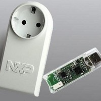
Manufacturer Part Number
OM13006,598
Description
BOARD EVAL EM773 METER EU PLUG
Manufacturer
NXP Semiconductors
Type
Other Power Managementr
Specifications of OM13006,598
Design Resources
Plug Meter Schematics, Gerber Files USB Dongle Schematics, Gerber Files
Main Purpose
Power Management, Energy/Power Meter
Embedded
Yes, MCU, 32-Bit
Utilized Ic / Part
EM773FHN33,551
Interface Type
USB
Maximum Operating Temperature
+ 150 C
Operating Supply Voltage
1.8 V to 3.6 V
Product
Power Management Development Tools
Lead Free Status / RoHS Status
Lead free / RoHS Compliant
Primary Attributes
-
Secondary Attributes
-
Lead Free Status / Rohs Status
Lead free / RoHS Compliant
For Use With/related Products
EM773, OL2381
Other names
568-6681


NXP Semiconductors
8.4 Functional description
UM10415
User manual
8.3.8 GPIO masked interrupt status register
8.3.9 GPIO interrupt clear register
8.4.1 Write/read data operation
Bits read HIGH in the GPIOnMIS register reflect the status of the input lines triggering an
interrupt. Bits read as LOW indicate that either no interrupt on the corresponding input
pins has been generated or that the interrupt is masked. GPIOMIS is the state of the
interrupt after masking. The register is read-only.
Table 86.
This register allows software to clear edge detection for port bits that are identified as
edge-sensitive in the Interrupt Sense register. This register has no effect on port bits
identified as level-sensitive.
Table 87.
In order for software to be able to set GPIO bits without affecting any other pins in a single
write operation, bits [13:2] of a 14-bit wide address bus are used to create a 12-bit wide
mask for write and read operations on the 12 GPIO pins for each port. Only GPIOnDATA
bits masked by 1 are affected by read and write operations. The masked GPIOnDATA
register can be located anywhere between address offsets 0x0000 to 0x3FFC in the
GPIOn address space. Reading and writing to the GPIOnDATA register at address
0x3FFC sets all masking bits to 1.
Write operation
Bit
11:0
31:12
Bit
11:0
31:12
Symbol Value Description
MASK
-
Symbol
CLR
-
GPIOnMIS register (GPIO0MIS, address 0x5000 8018 to GPIO3MIS, address
0x5003 8018) bit description
GPIOnIC register (GPIO0IC, address 0x5000 801C to GPIO3IC, address 0x5003
801C) bit description
All information provided in this document is subject to legal disclaimers.
0
1
-
Value
0
1
-
Rev. 1 — 10 September 2010
Selects interrupt on pin x to be masked (x = 0 to 11).
No interrupt or interrupt masked on pin PIOn_x.
Interrupt on PIOn_x.
Reserved
Description
Selects interrupt on pin x to be cleared (x = 0 to
11). Clears the interrupt edge detection logic. This
register is write-only.
Remark: The synchronizer between the GPIO and
the NVIC blocks causes a delay of 2 clocks. It is
recommended to add two NOPs after the clear of
the interrupt edge detection logic before the exit of
the interrupt service routine.
No effect.
Clears edge detection logic for pin PIOn_x.
Reserved
Chapter 8: EM773 General Purpose I/O (GPIO)
UM10415
© NXP B.V. 2010. All rights reserved.
Reset
value
0x00
-
0x00
-
Reset
value
Access
W
-
Access
R
-
69 of 310
Related parts for OM13006,598
Image
Part Number
Description
Manufacturer
Datasheet
Request
R

Part Number:
Description:
NXP Semiconductors designed the LPC2420/2460 microcontroller around a 16-bit/32-bitARM7TDMI-S CPU core with real-time debug interfaces that include both JTAG andembedded trace
Manufacturer:
NXP Semiconductors
Datasheet:

Part Number:
Description:
NXP Semiconductors designed the LPC2458 microcontroller around a 16-bit/32-bitARM7TDMI-S CPU core with real-time debug interfaces that include both JTAG andembedded trace
Manufacturer:
NXP Semiconductors
Datasheet:
Part Number:
Description:
NXP Semiconductors designed the LPC2468 microcontroller around a 16-bit/32-bitARM7TDMI-S CPU core with real-time debug interfaces that include both JTAG andembedded trace
Manufacturer:
NXP Semiconductors
Datasheet:
Part Number:
Description:
NXP Semiconductors designed the LPC2470 microcontroller, powered by theARM7TDMI-S core, to be a highly integrated microcontroller for a wide range ofapplications that require advanced communications and high quality graphic displays
Manufacturer:
NXP Semiconductors
Datasheet:
Part Number:
Description:
NXP Semiconductors designed the LPC2478 microcontroller, powered by theARM7TDMI-S core, to be a highly integrated microcontroller for a wide range ofapplications that require advanced communications and high quality graphic displays
Manufacturer:
NXP Semiconductors
Datasheet:
Part Number:
Description:
The Philips Semiconductors XA (eXtended Architecture) family of 16-bit single-chip microcontrollers is powerful enough to easily handle the requirements of high performance embedded applications, yet inexpensive enough to compete in the market for hi
Manufacturer:
NXP Semiconductors
Datasheet:
Part Number:
Description:
The XA-S3 device is a member of Philips Semiconductors? XA(eXtended Architecture) family of high performance 16-bitsingle-chip microcontrollers
Manufacturer:
NXP Semiconductors
Datasheet:

Part Number:
Description:
The NXP BlueStreak LH75401/LH75411 family consists of two low-cost 16/32-bit System-on-Chip (SoC) devices
Manufacturer:
NXP Semiconductors
Datasheet:
Part Number:
Description:
The NXP LPC3130/3131 combine an 180 MHz ARM926EJ-S CPU core, high-speed USB2
Manufacturer:
NXP Semiconductors
Datasheet:
Part Number:
Description:
The NXP LPC3141 combine a 270 MHz ARM926EJ-S CPU core, High-speed USB 2
Manufacturer:
NXP Semiconductors
Part Number:
Description:
The NXP LPC3143 combine a 270 MHz ARM926EJ-S CPU core, High-speed USB 2
Manufacturer:
NXP Semiconductors

Part Number:
Description:
The NXP LPC3152 combines an 180 MHz ARM926EJ-S CPU core, High-speed USB 2
Manufacturer:
NXP Semiconductors
Part Number:
Description:
The NXP LPC3154 combines an 180 MHz ARM926EJ-S CPU core, High-speed USB 2
Manufacturer:
NXP Semiconductors

Part Number:
Description:
Standard level N-channel enhancement mode Field-Effect Transistor (FET) in a plastic package using NXP High-Performance Automotive (HPA) TrenchMOS technology
Manufacturer:
NXP Semiconductors
Datasheet: