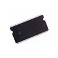
MT46V16M16P-5B:K Micron Technology Inc, MT46V16M16P-5B:K Datasheet - Page 38

MT46V16M16P-5B:K
Manufacturer Part Number
MT46V16M16P-5B:K
Description
DRAM Chip DDR SDRAM 256M-Bit 16Mx16 2.6V 66-Pin TSOP Tray
Manufacturer
Micron Technology Inc
Type
DDR SDRAMr
Datasheet
1.MT46V16M16P-5BK.pdf
(93 pages)
Specifications of MT46V16M16P-5B:K
Density
256 Mb
Maximum Clock Rate
400 MHz
Package
66TSOP
Address Bus Width
15 Bit
Operating Supply Voltage
2.6 V
Maximum Random Access Time
0.7 ns
Operating Temperature
0 to 70 °C
Organization
16Mx16
Address Bus
15b
Access Time (max)
700ps
Operating Supply Voltage (typ)
2.6V
Package Type
TSOP
Operating Temp Range
0C to 70C
Operating Supply Voltage (max)
2.7V
Operating Supply Voltage (min)
2.5V
Supply Current
260mA
Pin Count
66
Mounting
Surface Mount
Operating Temperature Classification
Commercial
Lead Free Status / RoHS Status
Compliant
Available stocks
Company
Part Number
Manufacturer
Quantity
Price
Company:
Part Number:
MT46V16M16P-5B:K
Manufacturer:
MICRON
Quantity:
6 589
Company:
Part Number:
MT46V16M16P-5B:K
Manufacturer:
MICRON
Quantity:
20 000
Company:
Part Number:
MT46V16M16P-5B:K
Manufacturer:
MICRON
Quantity:
7 580
PDF: 09005aef80768abb/Source: 09005aef82a95a3a
DDR_x4x8x16_Core2.fm - 256Mb DDR: Rev. O, Core DDR: Rev. B 1/09 EN
16. The CK/CK# input reference level (for timing referenced to CK/CK#) is the point at
17. Inputs are not recognized as valid until V
18. The output timing reference level, as measured at the timing reference point (indi-
19.
20. The intent of the “Don’t Care” state after completion of the postamble is the DQS-
21. This is not a device limit. The device will operate with a negative value, but system
22. It is recommended that DQS be valid (HIGH or LOW) on or before the WRITE com-
23. MIN (
24. The refresh period is 64ms (commerial and industrial) or 16ms (automotive). This
25. The I/O capacitance per DQS and DQ byte/group will not differ by more than this
26. The data valid window is derived by achieving other specifications:
27. Referenced to each output group: x4 = DQS with DQ0–DQ3; x8 = DQS with DQ0–DQ7;
28. This limit is actually a nominal value and does not result in a fail value. CKE is HIGH
29. To maintain a valid level, the transitioning edge of the input must:
29b. Reach at least the target AC level.
29a. Sustain a constant slew rate from the current AC level through to the target AC
29c. After the AC target level is reached, continue to maintain at least the target DC
which CK and CK# cross; the input reference level for signals other than CK/CK# is
V
refresh mode, V
period before V
cated in Note 3), is V
t
tions. These parameters are not referenced to a specific voltage level, but specify
when the device output is no longer driving (High-Z) or begins driving (Low-Z).
driven signal should either be HIGH, LOW, or High-Z, and that any signal transition
within the input switching region must follow valid input requirements. That is, if
DQS transitions HIGH (above V
V
performance could be degraded due to bus turnaround.
mand. The case shown (DQS going from High-Z to logic LOW) applies when no
WRITEs were previously in progress on the bus. If a previous WRITE was in progress,
DQS could be HIGH during this time, depending on
minimum absolute value for the respective parameter.
ments is the largest multiple of
equates to an average refresh rate of 7.8125µs (commercial and industrial) or 1.95us
(automotive). However, an AUTO REFRESH command must be asserted at least once
every 70.3µs(commerial and industrial) or 17.55µs (automotive); burst refreshing or
posting by the DRAM controller greater than 8 REFRESH cycles is not allowed.
maximum amount for any given device.
t
tion to the clock duty cycle and a practical data valid window can be derived. The
clock is allowed a maximum duty cycle variation of 45/55, because functionality is
uncertain when operating beyond a 45/55 ratio. The data valid window derating
curves are provided in Figure 12 on page 37 for duty cycles ranging between 50/50
and 45/55.
x16 = LDQS with DQ0–DQ7 and UDQS with DQ8–DQ15.
during the REFRESH command period (
standby).
HZ and
DQSQ, and
REF
IH
[
level, V
level, V
DC
.
t
RC or
] prior to
t
LZ transitions occur in the same access time windows as data valid transi-
IL
IL
t
t
(
(
RFC) for I
QH (
AC
DC
REF
REF
) or V
t
) or V
DQSH [MIN]).
t
QH =
stabilizes, CKE < 0.3 × V
must be powered within specified range. Exception: during the
TT
IH
IH
DD
.
(
(
t
AC
DC
HP -
measurements is the smallest multiple of
).
36
).
t
QHS). The data valid window derates in direct propor-
t
IH
CK that meets the maximum absolute value for
[
DC
Micron Technology, Inc., reserves the right to change products or specifications without notice.
] MIN) then it must not transition LOW (below
Electrical Specifications – DC and AC
t
REF
RFC [MIN]), else CKE is LOW (that is, during
DD
stabilizes. Once initialized, including self
256Mb: x4, x8, x16 DDR SDRAM
is recognized as LOW.
t
DQSS.
t
RAS (MAX) for I
©2003 Micron Technology, Inc. All rights reserved.
t
CK that meets the
t
HP (
DD
t
CK/2),
measure-
t
RAS.


