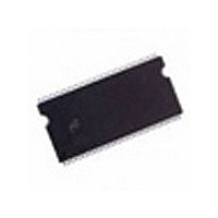
MT46V16M16P-5B:K Micron Technology Inc, MT46V16M16P-5B:K Datasheet - Page 46

MT46V16M16P-5B:K
Manufacturer Part Number
MT46V16M16P-5B:K
Description
DRAM Chip DDR SDRAM 256M-Bit 16Mx16 2.6V 66-Pin TSOP Tray
Manufacturer
Micron Technology Inc
Type
DDR SDRAMr
Datasheet
1.MT46V16M16P-5BK.pdf
(93 pages)
Specifications of MT46V16M16P-5B:K
Density
256 Mb
Maximum Clock Rate
400 MHz
Package
66TSOP
Address Bus Width
15 Bit
Operating Supply Voltage
2.6 V
Maximum Random Access Time
0.7 ns
Operating Temperature
0 to 70 °C
Organization
16Mx16
Address Bus
15b
Access Time (max)
700ps
Operating Supply Voltage (typ)
2.6V
Package Type
TSOP
Operating Temp Range
0C to 70C
Operating Supply Voltage (max)
2.7V
Operating Supply Voltage (min)
2.5V
Supply Current
260mA
Pin Count
66
Mounting
Surface Mount
Operating Temperature Classification
Commercial
Lead Free Status / RoHS Status
Compliant
Available stocks
Company
Part Number
Manufacturer
Quantity
Price
Company:
Part Number:
MT46V16M16P-5B:K
Manufacturer:
MICRON
Quantity:
6 589
Company:
Part Number:
MT46V16M16P-5B:K
Manufacturer:
MICRON
Quantity:
20 000
Company:
Part Number:
MT46V16M16P-5B:K
Manufacturer:
MICRON
Quantity:
7 580
Table 30:
PDF: 09005aef80768abb/Source: 09005aef82a95a3a
DDR_x4x8x16_Core2.fm - 256Mb DDR: Rev. O, Core DDR: Rev. B 1/09 EN
Current State
Any
Idle
Row active
Read
(auto precharge
disabled)
Write
(auto precharge
disabled)
Truth Table 3 – Current State Bank n – Command to Bank n
Notes: 1–6 apply to the entire table; Notes appear below
Notes:
CS#
H
L
L
L
L
L
L
L
L
L
L
L
L
L
L
1. This table applies when CKE
2. This table is bank-specific, except where noted (that is, the current state is for a specific
3. Current state definitions:
4. The following states must not be interrupted by a command issued to the same bank. COM-
5. The following states must not be interrupted by any executable command; COMMAND
after
bank and the commands shown are those allowed to be issued to that bank when in that
state). Exceptions are covered in the notes below.
MAND INHIBIT or NOP commands, or allowable commands to the other bank should be
issued on any clock edge occurring during these states. Allowable commands to the other
bank are determined by its current state and Table 30 and according to Table 31 on
page 45.
INHIBIT or NOP commands must be applied on each positive clock edge during these states.
• Idle: The bank has been precharged, and
• Row active: A row in the bank has been activated, and
• Read: A READ burst has been initiated, with auto precharge disabled, and has not yet
• Write: A WRITE burst has been initiated, with auto precharge disabled, and has not yet
• Precharging: Starts with registration of a PRECHARGE command and ends when
• Row activating: Starts with registration of an ACTIVE command and ends when
• Read with auto precharge enabled: Starts with registration of a READ command with
• Write with auto precharge enabled: Starts with registration of a WRITE command with
RAS# CAS#
bursts/accesses and no register accesses are in progress.
terminated or been terminated.
terminated or been terminated.
met. Once
met. Once
auto precharge enabled and ends when
will be in the idle state.
auto precharge enabled and ends when
will be in the idle state.
H
H
H
H
H
H
H
H
X
L
L
L
L
L
L
t
XSNR has been met (if the previous state was self refresh).
H
H
H
H
H
H
X
L
L
L
L
L
L
L
L
t
t
RP is met, the bank will be in the idle state.
RCD is met, the bank will be in the “row active” state.
WE#
X
H
H
H
H
H
H
L
L
L
L
L
L
L
L
Command/Action
DESELECT (NOP/continue previous operation)
NO OPERATION (NOP/continue previous operation)
ACTIVE (select and activate row)
AUTO REFRESH
LOAD MODE REGISTER
READ (select column and start READ burst)
WRITE (select column and start WRITE burst)
PRECHARGE (deactivate row in bank or banks)
READ (select column and start new READ burst)
WRITE (select column and start WRITE burst)
PRECHARGE (truncate READ burst, start PRECHARGE)
BURST TERMINATE
READ (select column and start READ burst)
WRITE (select column and start new WRITE burst)
PRECHARGE (truncate WRITE burst, start
PRECHARGE)
n-1
44
was HIGH and CKE
Micron Technology, Inc., reserves the right to change products or specifications without notice.
t
t
RP has been met. Once
RP has been met. Once
t
RP has been met.
256Mb: x4, x8, x16 DDR SDRAM
n
is HIGH (see Table 33 on page 47) and
t
RCD has been met. No data
©2003 Micron Technology, Inc. All rights reserved.
t
t
RP is met, the bank
RP is met, the bank
Commands
Notes
10, 12
10, 11
8, 11
t
10
10
10
10
t
RCD is
7
7
8
8
9
RP is


