MT46V16M16P-5B:K Micron Technology Inc, MT46V16M16P-5B:K Datasheet - Page 75

MT46V16M16P-5B:K
Manufacturer Part Number
MT46V16M16P-5B:K
Description
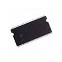
DRAM Chip DDR SDRAM 256M-Bit 16Mx16 2.6V 66-Pin TSOP Tray
Manufacturer
Micron Technology Inc
Type
DDR SDRAMr
Datasheet
1.MT46V16M16P-5BK.pdf
(93 pages)
Specifications of MT46V16M16P-5B:K
Density
256 Mb
Maximum Clock Rate
400 MHz
Package
66TSOP
Address Bus Width
15 Bit
Operating Supply Voltage
2.6 V
Maximum Random Access Time
0.7 ns
Operating Temperature
0 to 70 °C
Organization
16Mx16
Address Bus
15b
Access Time (max)
700ps
Operating Supply Voltage (typ)
2.6V
Package Type
TSOP
Operating Temp Range
0C to 70C
Operating Supply Voltage (max)
2.7V
Operating Supply Voltage (min)
2.5V
Supply Current
260mA
Pin Count
66
Mounting
Surface Mount
Operating Temperature Classification
Commercial
Lead Free Status / RoHS Status
Compliant
Available stocks
Company
Part Number
Manufacturer
Quantity
Price
Company:
Part Number:
MT46V16M16P-5B:K
Manufacturer:
MICRON
Quantity:
6 589
Company:
Part Number:
MT46V16M16P-5B:K
Manufacturer:
MICRON
Quantity:
20 000
Company:
Part Number:
MT46V16M16P-5B:K
Manufacturer:
MICRON
Quantity:
7 580
PDF: 09005aef80768abb/Source: 09005aef82a95a3a
DDR_x4x8x16_Core2.fm - 256Mb DDR: Rev. O, Core DDR: Rev. B 1/09 EN
Data for any WRITE burst may be concatenated with or truncated with a subsequent
WRITE command. In either case, a continuous flow of input data can be maintained.
The new WRITE command can be issued on any positive edge of clock following the
previous WRITE command. The first data element from the new burst is applied after
either the last element of a completed burst or the last desired data element of a longer
burst which is being truncated. The new WRITE command should be issued x cycles
after the first WRITE command, where x equals the number of desired data element
pairs (pairs are required by the 2n-prefetch architecture).
Figure 39 on page 75 shows concatenated bursts of 4. An example of nonconsecutive
WRITEs is shown in Figure 40 on page 76. Full-speed random write accesses within a
page or pages can be performed as shown in Figure 41 on page 76.
Data for any WRITE burst may be followed by a subsequent READ command. To follow a
WRITE without truncating the WRITE burst,
on page 77.
Data for any WRITE burst may be truncated by a subsequent READ command, as shown
in Figure 43 on page 78.
Note that only the data-in pairs that are registered prior to the
to the internal array, and any subsequent data-in should be masked with DM, as shown
in Figure 44 on page 79.
Data for any WRITE burst may be followed by a subsequent PRECHARGE command. To
follow a WRITE without truncating the WRITE burst,
Figure 45 on page 80.
Data for any WRITE burst may be truncated by a subsequent PRECHARGE command, as
shown in Figure 46 on page 81 and Figure 47 on page 82. Only the data-in pairs regis-
tered prior to the
should be masked with DM, as shown in Figures 46 and 47. After the PRECHARGE
command, a subsequent command to the same bank cannot be issued until
t
WR period are written to the internal array; any subsequent data-in
73
Micron Technology, Inc., reserves the right to change products or specifications without notice.
t
WTR should be met, as shown in Figure 42
256Mb: x4, x8, x16 DDR SDRAM
t
WR should be met, as shown in
©2003 Micron Technology, Inc. All rights reserved.
t
WTR period are written
Operations
t
RP is met.


