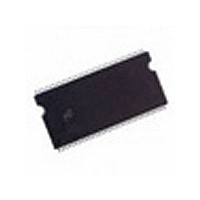
MT46V16M16P-5B:K Micron Technology Inc, MT46V16M16P-5B:K Datasheet - Page 61

MT46V16M16P-5B:K
Manufacturer Part Number
MT46V16M16P-5B:K
Description
DRAM Chip DDR SDRAM 256M-Bit 16Mx16 2.6V 66-Pin TSOP Tray
Manufacturer
Micron Technology Inc
Type
DDR SDRAMr
Datasheet
1.MT46V16M16P-5BK.pdf
(93 pages)
Specifications of MT46V16M16P-5B:K
Density
256 Mb
Maximum Clock Rate
400 MHz
Package
66TSOP
Address Bus Width
15 Bit
Operating Supply Voltage
2.6 V
Maximum Random Access Time
0.7 ns
Operating Temperature
0 to 70 °C
Organization
16Mx16
Address Bus
15b
Access Time (max)
700ps
Operating Supply Voltage (typ)
2.6V
Package Type
TSOP
Operating Temp Range
0C to 70C
Operating Supply Voltage (max)
2.7V
Operating Supply Voltage (min)
2.5V
Supply Current
260mA
Pin Count
66
Mounting
Surface Mount
Operating Temperature Classification
Commercial
Lead Free Status / RoHS Status
Compliant
Available stocks
Company
Part Number
Manufacturer
Quantity
Price
Company:
Part Number:
MT46V16M16P-5B:K
Manufacturer:
MICRON
Quantity:
6 589
Company:
Part Number:
MT46V16M16P-5B:K
Manufacturer:
MICRON
Quantity:
20 000
Company:
Part Number:
MT46V16M16P-5B:K
Manufacturer:
MICRON
Quantity:
7 580
Figure 25:
ACTIVE
PDF: 09005aef80768abb/Source: 09005aef82a95a3a
DDR_x4x8x16_Core2.fm - 256Mb DDR: Rev. O, Core DDR: Rev. B 1/09 EN
Extended Mode Register Definition
Notes:
1. n is the most significant row address bit from Table 2 on page 2.
2. The reduced drive strength option is available only on Design Revision F and K.
3. The QFC# option is not supported.
After a row is opened with an ACTIVE command, a READ or WRITE command may be
issued to that row, subject to the
the clock period and rounded up to the next whole number to determine the earliest
clock edge after the ACTIVE command on which a READ or WRITE command can be
entered. For example, a
results in 2.7 clocks rounded to 3. This is reflected in Figure 26 on page 60, which covers
any case where 2 <
same procedure is used to convert other specification limits from time units to clock
cycles).
A row remains active (or open) for accesses until a PRECHARGE command is issued to
that bank. A PRECHARGE command must be issued before opening a different row in
the same bank.
A subsequent ACTIVE command to a different row in the same bank can only be issued
after the previous active row has been “closed” (precharged). The minimum time
interval between successive ACTIVE commands to the same bank is defined by
A subsequent ACTIVE command to another bank can be issued while the first bank is
being accessed, which results in a reduction of total row-access overhead. The minimum
time interval between successive ACTIVE commands to different banks is defined by
t
Mn + 2
RRD.
0
0
1
1
Mn + 1
En
0
–
0
1
0
1
. . .
0
–
n + 2
Mode Register Definition
Base mode register
Extended mode register
Reserved
Reserved
BA1
E9
0
0
–
E8
n + 1
0
–
BA0
t
1
RCD (MIN)/
E7
0
–
n 1
An
E6
t
0
–
. . .
RCD specification of 20ns with a 133 MHz clock (7.5ns period)
. . .
Operating Mode
E5
0
–
9
A9
59
E4
0
–
8
A8
t
CK ≤ 3 (Figure 26 also shows the same case for
t
E3
RCD specification.
0
–
7
A7 A6 A5 A4 A3
E2
6
0
–
3
E1
Micron Technology, Inc., reserves the right to change products or specifications without notice.
0
1
5
E1, E0
2
Valid
–
4
Drive Strength
3
Reduced
Normal
E0
Operating Mode
0
1
256Mb: x4, x8, x16 DDR SDRAM
2
A2 A1 A0
DS
Reserved
Reserved
1
DLL
t
RCD (MIN) should be divided by
0
Disable
Enable
DLL
Address bus
Extended mode
register (Ex)
©2003 Micron Technology, Inc. All rights reserved.
Operations
t
RRD; the
t
RC.


